Table of Contents
Advertisement
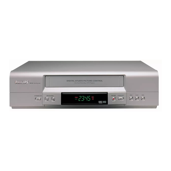
Video Cassette Recorder
Service
Service
Service
Service Manual
Contents
Chapter
Sec. 1:
Cabinet Disassembly Instructions
Schematic Diagrams and CBA's
Exploded Views
Mechanical and Electrical Parts Lists
Sec. 2:
Standard Maintenance
Mechanism Alignment Procedures
Disassembly / Assembly of Mechanism
Deck Exploded View
For technical data reference is made to the Service Manual of VR540/02/07/16
3103 785 22160. The present manual states only the differences.
Safety regulations require that the set be restored to its original
condition and that parts which are identical with those specified
be used.
Published by BK 2003 Video Service Department
VR140
/02
VR140
/07
VR140
/39
VR140
/58
Survey of versions:
/02
PAL B/G
/07
PAL I, Ireland
/16
PAL B/G, Spain
/39
SECAM L,L' & PAL B/G, I
/58
PAL/SECAM B/G, D/K
Printed in Japan
c Copyright reserved
VR840
/07
VR840
/16
VR840
/39
VR840
/58
Subject to modification
GB
3103 785 22180
Advertisement
Table of Contents

Related Manuals for Philips VR140/02


Summary of Contents for Philips VR140/02
- Page 1 Video Cassette Recorder VR140 VR840 Service VR140 VR840 Service VR140 VR840 Service VR140 VR840 Service Manual Contents Survey of versions: PAL B/G Chapter PAL I, Ireland PAL B/G, Spain Sec. 1: Cabinet Disassembly Instructions SECAM L,L' & PAL B/G, I Schematic Diagrams and CBA's Exploded Views PAL/SECAM B/G, D/K...
-
Page 2: Operating Controls And Functions
To access or remove the VCR’s on- [ VR140/ (39, 58) ] screen status display. To exit on-screen menus. Or, to To change the video (colour) system. access or remove a status display or menu of Philips To call up main menu of VCR. MENU PLAY To play a tape, select an item in the menu 0..9... - Page 3 PLAY To play a tape. STOP/EJECT To stop the tape and eject the cassette. Back of the set VR140/02, VR140/07, VR140/58 A E R I A L R F O U T VR140/39 AV2 (DECODER) AV1 (TV)
- Page 4 To switch VCR or Philips TV on or off, interrupt menu function. STATUS/EXIT To access or remove the VCR’s on-screen status display. To exit on-screen menus. Or, to access or remove a status display or menu of Philips TV. 0..9 Press to select channels at VCR or Philips TV.
- Page 5 Front of the device STANDBY/ON STOP/EJECT PROGRAMME PWR. RECORD PLAY A/V FRONT CONNECTORS To switch off or on, interrupt a function. STANDBY/ON PROGRAMME+ PROGRAMME- To select the programme number. During normal or slow motion playback, press to adjust the tracking. RECORD To record the TV channel selected at this moments.
-
Page 6: Signal Name Abbreviations
SIGNAL NAME ABBREVIATIONS [ VR140/ (02, 07, 39, 58), VR840/ (07, 16, 39, 58) ] Signal Name Function Signal Name Function Capstan Motor C-FG Rotation Detection 4.43MHz 4.43MHz Clock Pulse SCART 1 8Pin Output Control 8POUT-1 C-POW-SW Capstan Power Switching Signal Signal C-POWER- Control SCART 1 8Pin Level by... - Page 7 Signal Name Function Signal Name Function Hi-Fi-A (R) Hi-Fi Audio Head (R) REMOCON-IN Remote Control Sensor Hi-Fi-COM Hi-Fi Audio Head Common RESET System Reset Signal (Reset=”L”) HiFi-H-SW HiFi Audio Head Switching Pulse RESET +5V +5V at System Reset Signal LPF Connected Terminal (Slicer) RF-SW Video Head Switching Pulse RGB-...
-
Page 8: Disassembly Flowchart
CABINET DISASSEMBLY INSTRUCTIONS [ VR140/ (02,07,39,58) ] 1. Disassembly Flowchart (1): Identification (location) No. of parts in the figures (2): Name of the part This flowchart indicates the disassembly steps to gain (3): Figure Number for reference access to item(s) to be serviced. When reassembling, (4): Identification of parts to be removed, unhooked, follow the steps in reverse order. -
Page 9: Top View
(L-2) [4] Jack CBA (L-2) (S-5) Desolder Fig. 4 [2] Front Assembly [7] Cylinder Shield Cylinder Assembly (L-1) Fig. 2 FE Head (S-7) AC Head (S-2) Assembly (S-3) (S-2) (S-2) (S-4) [3]VCR Chassis Unit (S-3) [5] Deck Assembly (S-2) [6] Main CBA (S-6) (S-6) TOP VIEW... - Page 10 SW507 LD-SW [6] Main CBA [5] Deck Assembly Cam Gear Hole Shaft Hole LD-SW [6] Main CBA Fig. 6 1-7-6 HE270DC...
- Page 11 [ VR840/ (07, 16, 39, 58) ] 1. Disassembly Flowchart (1): Identification (location) No. of parts in the figures (2): Name of the part This flowchart indicates the disassembly steps to gain (3): Figure Number for reference access to item(s) to be serviced. When reassembling, (4): Identification of parts to be removed, unhooked, follow the steps in reverse order.
- Page 12 (L-2) [4] Jack CBA (S-5) Desolder [2] Front Assembly (L-2) Fig. 4 (L-1) Fig. 2 (S-2) (S-2) (S-3) (S-3) (S-2) (S-4) (S-3) (S-2) (S-3) [3]VCR Chassis Unit (S-3) Fig. 3 1-7-8 HE490DC...
- Page 13 Cylinder Assembly [7] Cylinder Shield (S-7) FE Head AC Head Assembly SW507 LD-SW [8] Rear Panel [6] Main CBA (L-3) [5] Deck Assembly [5] Deck Assembly Cam Gear [6] Main CBA Hole (S-6) Shaft Hole LD-SW [6] Main CBA (S-6) Fig.
-
Page 14: Block Diagrams
2. PREFIX SYMBOL "CL" MEANS WIRE-SOLDER " " = SMD Model Mark HOLES OF THE PCB. :USED TO INDICATE A TEST POINT WITH A TEST PIN. (WIRE IS SOLDERED DIRECTLY.) VR140/02 IC501 AL+5V TP501 VR140/07 (SERVO/SYSTEM CONTROL) MAIN CBA VR140/39... - Page 15 :INDICATES A TEST POINT WITH A JUMPER WIRE ACROSS A HOLE IN THE PCB. (CAN DISCONNECT AND RECONNECT.) :USED TO INDICATE A TEST POINT WITH A COMPONENT LEAD ON FOIL SIDE. VR140/02 2. PREFIX SYMBOL "CL" MEANS WIRE-SOLDER :USED TO INDICATE A TEST POINT WITH NO TEST PIN.
- Page 16 A-OUT2(R) A-OUT2 A-OUT2(L) TUNER Q152 PB/EE BUFFER Comparison Chart of Models & Marks AUDIO-SW-1 TO SERVO/SYSTEM Model Mark AUDIO-SW-2 CONTROL BLOCK VR140/02 VR140/07 IC301 (AUDIO SIGNAL PROCESS) VR140/39 TUNER J982 VR140/58 VR840/07 VR840/16 PB-ON VR840/39 LINE MUTE VR840/58 (DECK ASSEMBLY)
- Page 17 :INDICATES A TEST POINT WITH A JUMPER WIRE ACROSS A HOLE IN THE PCB. (CAN DISCONNECT AND RECONNECT.) :USED TO INDICATE A TEST POINT WITH A COMPONENT LEAD ON FOIL SIDE. VR140/02 2. PREFIX SYMBOL "CL" MEANS WIRE-SOLDER " " = SMD :USED TO INDICATE A TEST POINT WITH NO TEST PIN.
- Page 18 SIF OUT IF SIGNAL TU-AUDIO(L) 5 PROCESS TU-AUDIO 1 AUDIO OUT Comparison Chart of Models & Marks IC451 (Hi-Fi AUDIO SIGNAL PROCESS) Model Mark MUTE-ON VR140/02 VR140/07 R,S,U OUTPUT VR140/39 AUDIO IN MUTE SELECT VR140/58 VR840/07 MUTE-ON VR840/16 VR840/39 IIC-BUS SDA...
- Page 19 GND as a common terminal. Model Mark circuit are not defective before you connect the AC plug to the AC power supply. Otherwise it may cause some components in the power supply circuit to fail. VR140/02 VR140/07 VR140/39 MAIN CBA VR140/58 VR840/07 HOT CIRCUIT.
- Page 20 [ VR140/ (02, 17, 39, 58), VR840/ (07, 16, 39, 58) ] Main 1/8 Schematic Diagram Parts Location Guide Ref No. Position Ref No. Position Ref No. Position CAPACITORS CONNECTORS RESISTORS C501 CL502 R526 C502 CL504 R527 C506 DIODES R528 C508 D501 R529...
- Page 21 2.90 ~ 3.60V S-INH ------------------- ------------------- 3.60 ~ 4.30V ------------------- ------------------- ------------------- 4.30 ~ 5.00V KEY OFF KEY OFF KEY OFF Comparison Chart of Models and Marks MODEL MARK VR140/02 VR140/07 VR140/39 VR140/58 VR840/07 VR840/16 VR840/39 VR840/58 1-10-32 1-10-33 HE270SCM1...
- Page 22 Comparison Chart of MODE: SP/REC “ “ = SMD PLAY MODE Models and Marks REC MODE MODEL MARK (2.5) VR140/02 INDICATES THAT THE VOLTAGE THE SAME VOLTAGE FOR VR140/07 IS NOT CONSISTENT HERE. BOTH PLAY & REC MODES. VR140/39 VR140/58 VR840/07 VR840/16...
- Page 23 MAIN 2/8 Schematic Diagram Parts Location Guide Ref No. Position Ref No. Position CAPACITORS RESISTORS C538 R535 C540 R536 C561 R537 C562 R538 C701 R539 C702 R540 C703 R541 C704 R542 C706 R543 C707 R544 C708 R545 C709 R546 C710 R547 C712 R548...
- Page 24 MAIN 3/8 Schematic Diagram Parts Location Guide Ref No. Position Ref No. Position Ref No. Position Ref No. Position CAPACITORS CAPACITORS TRANSISTORS RESISTORS C251 C352 Q402 R403 C252 C401 Q403 R404 C253 C402 Q405 R407 C254 C403 Q406 R408 C302 C404 Q771 R409...
- Page 25 “ “ = SMD PLAY MODE Models and Marks REC MODE (2.5) MODEL MARK THE SAME VOLTAGE FOR INDICATES THAT THE VOLTAGE VR140/02 IS NOT CONSISTENT HERE. VR140/07 BOTH PLAY & REC MODES. VR140/39 VR140/58 VR840/07 VR840/16 VR840/39 VR840/58 1-10-38...
- Page 26 Comparison Chart of MODE: SP/REC “ “ = SMD PLAY MODE Models and Marks REC MODE (2.5) MODEL MARK VR140/02 INDICATES THAT THE VOLTAGE THE SAME VOLTAGE FOR VR140/07 IS NOT CONSISTENT HERE. BOTH PLAY & REC MODES. VR140/39 VR140/58 VR840/07 VR840/16...
- Page 27 MAIN 4/8 Schematic Diagram Parts Location Guide Ref No. Position Ref No. Position Ref No. Position CAPACITORS DIODES RESISTORS C151 D153 R153 C152 D154 R154 C153 D155 R155 C154 D156 R158 C155 D157 R756 C156 R757 C157 IC151 R758 C158 TRANSISTORS R759 C159...
- Page 28 MAIN 5/8 Schematic Diagram Parts Location Guide Ref No. Position Ref No. Position Ref No. Position CAPACITORS DIODES RESISTORS C002 D021 R008 C003 D023 AA-1 R009 C004 D051 BB-3 R011 C005 D052 CC-3 R012 C006 D053 BB-2 R013 C007 D055 CC-3 R014 C008...
- Page 29 Comparison Chart of Models and Marks MODEL MARK CAUTION ! CAUTION ! VR140/02 MODE: SP/REC PLAY MODE For continued protection against fire hazard, Fixed voltage ( or Auto voltage selectable ) power supply circuit is used in this unit. VR140/07...
- Page 30 Main 6/8 Schematic Diagram ( R, S, T, U ) Comparison Chart of Models and Marks MODEL MARK VR140/02 VR140/07 VR140/39 VR140/58 VR840/07 VR840/16 VR840/39 VR840/58 “ “ = SMD MODE: SP/REC PLAY MODE REC MODE (2.5) THE SAME VOLTAGE FOR INDICATES THAT THE VOLTAGE IS NOT CONSISTENT HERE.
- Page 31 Comparison Chart of Models and Marks MODE: SP/REC MODEL MARK “ “ = SMD PLAY MODE REC MODE VR140/02 (2.5) VR140/07 THE SAME VOLTAGE FOR INDICATES THAT THE VOLTAGE VR140/39 IS NOT CONSISTENT HERE. BOTH PLAY & REC MODES. VR140/58...
- Page 32 Main 8/8 Schematic Diagram ( R, S, T, U ) Comparison Chart of Models and Marks MODEL MARK MODE: SP/REC “ “ = SMD PLAY MODE VR140/02 REC MODE (2.5) VR140/07 INDICATES THAT THE VOLTAGE THE SAME VOLTAGE FOR VR140/39 BOTH PLAY & REC MODES. IS NOT CONSISTENT HERE.
- Page 33 PLAY MODE REC MODE Models and Marks (2.5) MODEL MARK THE SAME VOLTAGE FOR INDICATES THAT THE VOLTAGE IS NOT CONSISTENT HERE. BOTH PLAY & REC MODES. VR140/02 VR140/07 VR140/39 VR140/58 VR840/07 VR840/16 VR840/39 VR840/58 AFV Schematic Diagram Parts Location Guide Ref No.
- Page 34 Main CBA Parts Location Guide Ref No. Position Ref No. Position Ref No. Position Ref No. Position Ref No. Position Ref No. Position Ref No. Position Ref No. Position Ref No. Position Ref No. Position Ref No. Position CAPACITORS CAPACITORS CAPACITORS CAPACITORS CONNECTORS...
- Page 35 Main CBA Top View CAUTION ! CAUTION ! BECAUSE A HOT CHASSIS GROUND IS PRESENT IN THE POWER For continued protection against fire hazard, Fixed voltage ( or Auto voltage selectable ) power supply circuit is used in this unit. SUPPLY CIRCUIT , AN ISOLATION TRANSFORMER MUST BE USED.
- Page 36 Main CBA Bottom View CAUTION ! BECAUSE A HOT CHASSIS GROUND IS PRESENT IN THE POWER CAUTION ! For continued protection against fire hazard, SUPPLY CIRCUIT , AN ISOLATION TRANSFORMER MUST BE USED. Fixed voltage ( or Auto voltage selectable ) power supply circuit is used in this unit. replace only with the same type fuse.
- Page 37 Jack CBA Top View Jack CBA Parts Location Guide Ref No. Position Ref No. Position CAPACITORS TRANSISTORS C101 Q102 C102 RESISTORS C103 R101 C104 R102 C105 R103 C107 R104 C108 R105 C109 R106 C110 R108 C111 R109 C112 R110 C113 R111 C115 R112...
- Page 38 AFV CBA Top View ( R, S, T, U ) AFV CBA Bottom View ( R, S, T, U ) Comparison Chart of Models and Marks MODEL MARK VR140/02 VR140/07 VR140/39 VR140/58 AFV CBA Parts Location Guide VR840/07 Ref No.
-
Page 39: Wiring Diagram
Models & Marks (CAN DISCONNECT AND RECONNECT.) IN (R) IN (L) ANT-IN ANT-OUT 2. PREFIX SYMBOL "CL" MEANS WIRE-SOLDER Model Mark HOLES OF THE PCB. VR140/02 (WIRE IS SOLDERED DIRECTLY.) CN701 VR140/07 1 TU-AUDIO VR140/39 SENSOR CBA 3 GND VR140/58 (BHB300F01014) -
Page 40: System Control Timing Charts
SYSTEM CONTROL TIMING CHARTS [ VR140/ (02, 07, 39, 58), VR840/ (07, 16, 39, 58) ] Mode SW : LD-SW LD-SW Position detection A/D Input voltage Limit Symbol (Calculated voltage) 3.76V~4.50V (4.12V) 4.51V~5.00V (5.00V) 0.00V~0.25V (0.00V) 1.06V~1.50V (1.21V) 0.66V~1.05V (0.91V) 1.99V~2.60V (2.17V) 1.51V~1.98V... - Page 41 [ VR140/ (02,07,39,58) ] EJECT ST-S/ END-S "OFF" CASS.LOAD LD-FWD 0.2S LD-REV 0.7S LD-FWD 0.4S LD-FWD 0.5S LD-REV STOP(A) PLAY LD-FWD PLAY LD-FWD LD-REV 0.2S LD-FWD PLAY PLAY PAUSE STILL PAUSE NOISE CANCEL PAUSE STILL PAUSE NOISE CANCEL PAUSE STILL PLAY PLAY STOP...
- Page 42 STOP(A) STOP LD-REV 0.2S LD-FWD STOP /EJECT LD-FWD 2.5S LD-FWD 0.5S LD-REV STOP(A) LD-REV 0.2S LD-FWD STOP /EJECT LD-FWD 2.5S LD-FWD 0.5S LD-REV STOP(A) LD-FWD PAUSE LD-FWD 2.5S Short REV LD-REV 0.2S LD-FWD REC PAUSE REC or PAUSE STOP /EJECT LD-FWD 1.0S LD-REV...
- Page 43 [ VR840/ (07, 16, 39, 58) ] Still/Slow Control Frame Advance Timing Chart 1) SP Mode 18 RF-SW The first rise of RF-SW after a rise in F-AD signal F-AD (Internal Signal) "H" "H" "Z" C-DRIVE "L" "L" Stop detection (T2) Acceleration Detection (T1) Slow Tracking Value PB CTL...
- Page 44 2) LP/SLP Mode 18 RF-SW The first rise of RF-SW after a rise in F-AD signal F-AD (Internal Signal) "H" "H" "Z" C-DRIVE "L" "L" Stop detection (T2) Acceleration Detection (T1) Slow Tracking Value PB CTL Reversal Limit Value 20ms 78 C-F/R 16 H-A-SW 15 ROTA...
- Page 45 EJECT ST-S/ END-S "OFF" CASS.LOAD LD-FWD 0.2S LD-REV 0.7S LD-FWD 0.4S LD-FWD 0.5S LD-REV STOP(A) PLAY LD-FWD PLAY LD-FWD LD-REV 0.2S LD-FWD PLAY PLAY PAUSE (SLOW) LD-FWD STILL(SLOW) PLAY LD-REV 0.2S LD-FWD PLAY STOP /EJECT LD-REV STOP(A) Fig. 5 1-13-11 HE270TI...
- Page 46 STOP(A) STOP LD-REV 0.2S LD-FWD STOP /EJECT LD-FWD 2.5S LD-FWD 0.5S LD-REV STOP(A) LD-REV 0.2S LD-FWD STOP /EJECT LD-FWD 2.5S LD-FWD 0.5S LD-REV STOP(A) LD-FWD PAUSE LD-FWD 2.5S Short REV LD-REV 0.2S LD-FWD REC PAUSE REC or PAUSE STOP /EJECT LD-FWD 1.0S LD-REV...
-
Page 47: Ic Pin Function Descriptions
[ VR140/ (02, 07, 39, 58), VR840/ (07, 16, 39, 58) ] Comparison Chart of Models and Marks Signal Active Mark Function Name Level Model Mark N.U. Not Used VR140/02 OUT D-V- Dummy V-sync H/Hi-z SYNC Output VR140/07 REMOC Remote VR140/39 ON-IN Control Sensor... - Page 48 Signal Active Signal Active Mark Function Mark Function Name Level Name Level N,O, N.U. Not Used Q,R, N.U. Not Used OUT OSD-V- OSD Video S,T,U Signal Output OUT AUDIO- Audio IN/OUT OSDVc Control Signal SW-1 OSDVcc N,O, LPF Connected Q,R, N.U.
- Page 49 Signal Active Signal Active Mark Function Mark Function Name Level Name Level LED Clock Capstan Motor OUT DRV- Driver IC Rotation PULSE DATA C-FG Control Data Detection Pulse LED Clock OUT DRV- Driver IC Chip N.U. Not Used Select Signal N.U.
-
Page 50: Lead Identifications
LEAD IDENTIFICATIONS [ VR140/ (02, 07, 39, 58), VR840/ (07, 16, 39, 58) ] 2SC1815-BL(TPE2) LM339DT BN1L4M-T 2SC1815-Y(TPE2) KIA339F EL BN1F4M-T 2SC1815-GR(TPE2) BA1F4M-T 2SC3266-Y (TPE2) KTA1266(GR) 2SC2120-Y(TPE2) KTC3199(Y,GR,BL) KTC3203(Y) 2SC2785(J.H.F.K) 2SC1815-BL(TPE2) KRA103M 2SA1020(Y) KRC103M KTC3205(Y) KRA104M 2SA1015-GR(TPE2) KTA1281(Y) LA71750AM-MTB QSZAD0RMB141 QSZAC0RMB144 E C B E C B... -
Page 51: Electrical Parts List
PRODUCT SAFETY NOTE: Products marked with a h have special characteristics important to safety. Before replacing any of these components, read carefully the product safety notice in this service manual. Don't degrade the safety of the product through improper servicing. NOTES: Parts that not assigned part numbers (-----------) are not available. - Page 52 ELECTRICAL PARTS LIST Pos. 12 NC Description C252 CHIP CERAMIC CAP. B K 1000PF/50V C253 ELECTROLYTIC CAP. 1UF/50V M H7 C254 CHIP CERAMIC CAP. F Z 0.1UF/25V C302 CHIP CERAMIC CAP. B K 0.022UF/25V C303 ELECTROLYTIC CAP. 1UF/50V M H7 C304 ELECTROLYTIC CAP.
- Page 53 ELECTRICAL PARTS LIST Pos. 12 NC Description C402 ELECTROLYTIC CAP. 220UF/6.3V M H7 C403 CERAMIC CAP. B K 470PF/100V C404 FILM CAP.(P) 0.018UF/100V J C411 CHIP CERAMIC CAP. CG J 820PF/50V C412 CHIP CERAMIC CAP. B K 1800PF/50V C414 CHIP CERAMIC CAP. B K 0.01UF/50V C415 ELECTROLYTIC CAP.
- Page 54 ELECTRICAL PARTS LIST Pos. 12 NC Description C510 ELECTROLYTIC CAP. 22UF/10V M H7 C511 ELECTROLYTIC CAP. 100UF/6.3V H7 C512 CHIP CERAMIC CAP. F Z 0.1UF/25V C513 CHIP CERAMIC CAP. CG J 22PF/50V C514 CHIP CERAMIC CAP. CG J 22PF/50V C515 CHIP CERAMIC CAP.
- Page 55 ELECTRICAL PARTS LIST Pos. 12 NC Description C853 CHIP CERAMIC CAP. B K 4700PF/50V C854 CHIP CERAMIC CAP. B K 0.01UF/50V C855 CHIP CERAMIC CAP. F Z 0.1UF/25V C856 CHIP CERAMIC CAP. CG J 180PF/50V C858 CHIP CERAMIC CAP. CG J 560PF/50V C859 ELECTROLYTIC CAP.
- Page 56 ELECTRICAL PARTS LIST Pos. 12 NC Description IC771 9965 000 12184 IC:COMPARATOR KIA339F EL COILS L001 4822 526 10685 BEAD CORE B16 RH 3.5X10X1.3 L002 4822 526 10685 BEAD CORE B16 RH 3.5X10X1.3 L003 9965 000 13005 LINE FILTER 56MH TLF14CB5630R2 L009 9965 000 05627 CHOKE COIL 47UH-K...
- Page 57 ELECTRICAL PARTS LIST Pos. 12 NC Description R006 METAL OXIDE FILM RES. 1W J 1.8 OHM R007 CARBON RES. 1/4W J 22K OHM R008 CARBON RES. 1/4W J 100K OHM R009 CARBON RES. 1/4W G 3.3K OHM R011 CARBON RES. 1/4W J 390K OHM R012 CARBON RES.
- Page 58 ELECTRICAL PARTS LIST Pos. 12 NC Description R318 CHIP RES.(1608) 1/10W J 4.7K OHM R319 CHIP RES.(1608) 1/10W J 10K OHM R320 CHIP RES.(1608) 1/10W J 1K OHM R321 CARBON RES. 1/4W J 33 OHM R322 CHIP RES.(1608) 1/10W J 75 OHM R323 CARBON RES.
- Page 59 ELECTRICAL PARTS LIST Pos. 12 NC Description R461 CHIP RES.(1608) 1/10W J 10K OHM R462 CHIP RES.(1608) 1/10W J 2.7K OHM R463 CHIP RES.(1608) 1/10W J 8.2K OHM R464 CHIP RES.(1608) 1/10W J 39K OHM R465 CHIP RES.(1608) 1/10W J 8.2K OHM R466 CHIP RES.(1608) 1/10W J 5.6K OHM R467...
- Page 60 ELECTRICAL PARTS LIST Pos. 12 NC Description R549 CHIP RES.(1608) 1/10W J 1.2K OHM R551 CHIP RES.(1608) 1/10W J 100 OHM R552 CHIP RES.(1608) 1/10W J 10K OHM R555 CHIP RES.(1608) 1/10W J 10K OHM R556 CHIP RES.(1608) 1/10W J 10K OHM R557 CHIP RES.(1608) 1/10W J 10K OHM R558...
- Page 61 ELECTRICAL PARTS LIST Pos. 12 NC Description SW506 9965 000 16625 LEAF SWITCH MXS01830MVP0 SW507 9965 000 16626 ROTARY MODE SWITCH SSS-50MD SW509 4822 276 13954 TACT SWITCH KSM0614B SW510 4822 276 13954 TACT SWITCH KSM0614B SW511 4822 276 13954 TACT SWITCH KSM0614B SW512 4822 276 13954...
- Page 62 ELECTRICAL PARTS LIST Pos. 12 NC Description C112 CHIP CERAMIC CAP. CG J 470PF/50V C113 CHIP CERAMIC CAP. B K 2200PF/50V C115 ELECTROLYTIC CAP. 100UF/16V M H7 C116 ELECTROLYTIC CAP. 470UF/6.3V M C117 ELECTROLYTIC CAP. 470UF/6.3V M DIODES D101 9965 000 12178 ZENER DIODE DZ-11BSAT265 D102 9965 000 12178...
- Page 63 ELECTRICAL PARTS LIST Pos. 12 NC Description CAPACITORS CHIP CERAMIC CAP. F Z 0.1UF/25V CHIP CERAMIC CAP. CG J 56PF/50V CHIP CERAMIC CAP. CG J 22PF/50V CHIP CERAMIC CAP. CG J 56PF/50V CHIP CERAMIC CAP. CH C 3PF/50V CHIP CERAMIC CAP. CH C 3PF/50V CHIP CERAMIC CAP.
-
Page 64: Exploded Views
EXPLODED VIEWS [ VR140/ (02, 07, 39, 58), VR840/ (07, 16, 39, 58) ] Front Panel VR140/ (02, 07, 39, 58) VR840/ (07, 16, 39, 58) 1-17-4 HE270FEX... - Page 65 [ VR140/ (02, 07, 39, 58), VR840/ (07, 16, 39, 58) ] Cabinet 2L011 2L011 2B18 Comparison Chart of 2L011 Models and Marks Model Mark VR140/02 VR140/07 VR140/39 2L011 VR140/58 2B10 VR840/07 VR840/16 VR840/39 [ R,S,T,U ] VR840/58 2B10 JACK CBA...
-
Page 66: Mechanical Parts List
PRODUCT SAFETY NOTE: Products marked with a h have special characteristics important to safety. Before replacing any of these components, read carefully the product safety notice in this service manual. Don’t degrade the safety of the product through improper servicing. MECHANICAL PARTS LIST Pos. - Page 67 X20A X20B X45B X45C X45A [ N ] [ P,T ] [ O,R ] Unit Comparison Chart of Models and Marks Model Mark VR140/02 VR140/07 VR140/39 VR140/58 VR840/07 VR840/16 VR840/39 Some Ref. Numbers are not in sequence. VR840/58 1-17-6 HE270PEX...
-
Page 68: Standard Maintenance
STANDARD MAINTENANCE [ VR140/ (02, 07, 39, 58), VR840/ (07, 16, 39, 58) ] Service Schedule of Components [ VR140/ (02,07,39,58) ] H: Hours : Check I: Change Deck Periodic Service Schedule Ref.No. Part Name 1,000 H 2,000 H 3,000 H 4,000 H Cylinder Assembly Loading Motor Assembly... - Page 69 [ VR840/ (07,16,39,58) ] H: Hours : Check I: Change Deck Periodic Service Schedule Ref.No. Part Name 1,000 H 2,000 H 3,000 H 4,000 H Cylinder Assembly Loading Motor Assembly Pulley Assembly B587 Tension Lever Assembly AC Head Assembly B573,B574 Reel S, Reel T Capstan Motor Cap Belt...
- Page 70 Cleaning Cleaning of Audio Control Head Clean the head with a cotton swab. Cleaning of Video Head Procedure Clean the head with a head cleaning stick or chamois 1.Remove the top cabinet. cloth. 2.Dip the cotton swab in 90% isopropyl alcohol and Procedure clean the audio control head.
-
Page 71: Disassembly / Assembly Procedures Of Deck Mechanism
DISASSEMBLY/ASSEMBLY PROCEDURES OF DECK MECHANISM [ VR140/ (02, 07, 39, 58) ] Before following the procedures described below, be sure to remove the deck assembly from the cabinet. (Refer to CABINET DISASSEMBLY INSTRUCTIONS.) All the following procedures, including those for adjustment and replacement of parts, should be done in Eject mode;... - Page 72 REMOVAL INSTALLATION STEP START- REMOVE/*UNHOOK/ /LOC. PART ADJUSTMENT Fig. No. UNLOCK/RELEASE/ CONDITION UNPLUG/DESOLDER Loading Arm (SP) (+)Refer to Alignment [32] [25] DM2,DM14 Assembly Sec.Pg.2-4-24 Loading Arm (TU) (+)Refer to Alignment [32] [33] DM2,DM14 Assembly Sec.Pg.2-4-24 [34] [2],[25] M Brake (TU) Assembly DM1,DM15 *(P-7), Brake Belt [35] [2],[25] M Brake (SP) Assembly...
-
Page 73: Top View
Top View [41] [42] [46] [43] [14] [13] [11] [15] [36] [10] [12] [35] [34] [40] [29] [30] [16] [39] [38] Fig. DM1 Bottom View [20] [33] [32] [24] [26] [27] [25] [23] [28] [22] [21] [31] Fig. DM2 2-4-11 HE270DA... - Page 74 (S-1) (S-1) (L-1) (L-3) (L-2) (P-1) Fig. DM5 [46] Fig. DM3 [47] Pin D (L-14) Pin C Pull up Slide Pin A Pin B Slot A (S-2) Slots B Slot A First, while pushing the locking tab as shown at right, slide and pull up the right side on [2] to release Pin A and Pin B from the slots A.
- Page 75 (S-4) (S-5) [14] (S-6) [16] [15] Desolder from bottom (S-3) Lead with White Stripe Belt View for A Fig. DM7 Fig. DM9 Adj. Screw [11] [18] (L-4) (L-5) (P-3) [17] [13] [19] [12] (P-4) [10] (P-2) (S-7) Pin of [12] Pin of [10] Fig.
- Page 76 [22] (C-4) (S-8) (C-1) [23] (L-6) [21] (P-5) [20] Cap Belt (P-5) [28] Fig. DM11 When installing [23], install the spring (P-5) to [28] as shown in the left figure, and then install [23] while Pin on pressing the spring (P-5) to bottom the direction of the arrow in of [23]...
- Page 77 (P-6) [25] [31] Refer to the Alignment (C-3) Section, Page 2-4-24. (S-9) [29] [33] [30] (L-11) [32] (L-10) (L-8) (C-2) [27] [28] [24] [26] (L-9) Fig. DM14 Position of Mode Lever when installed [36] Break belt Pin of [35] (P-7) Pin of [31] Pin of [34] [34]...
- Page 78 [42] [41] [43] (L-13) Fig. DM16 [44] [45] Slide Fig. DM17 2-4-16 HE270DA...
- Page 79 [ VR840/ (07, 16, 39, 58) ] Before following the procedures described below, be sure to remove the deck assembly from the cabinet. (Refer to CABINET DISASSEMBLY INSTRUCTIONS.) All the following procedures, including those for adjustment and replacement of parts, should be done in Eject mode;...
- Page 80 REMOVAL INSTALLATION STEP START- REMOVE/*UNHOOK/ /LOC. PART ADJUSTMENT Fig. No. UNLOCK/RELEASE/ CONDITION UNPLUG/DESOLDER M Brake (TU) Assembly [36] [16],[26] DM1,DM15 (HI) M Brake (SP) Assembly [37] [2],[26] DM1,DM15 *(P-6) (HI) [38] [37] Tension Lever Assembly DM1,DM15 [39] [38] T Lever Holder DM15 *(L-10) [40]...
- Page 81 Top View [44] [45] [49] [46] [14] [13] [11] [15] [38] [10] [12] [37] [36] [43] [32] [41] [31] [40] [42] Fig. DM1 Bottom View [19] [35] [34] [25] [23] [24] [26] [27] [22] [28] [20] [33] Fig. DM2 2-4-19 HE490DA...
- Page 82 (S-1) (S-1) (L-1) (L-3) (L-2) (P-1) Fig. DM5 [49] Fig. DM3 [50] Pin D (L-12) Pin C Pull up Slide Pin A Pin B Slot A (S-2) Slots B Slot A First, while pushing the locking tab as shown in the right, slide and pull up the right side on [2] to release Pin A and Pin B from the slots A.
- Page 83 (S-4) (S-5) [14] (S-6) [15] Desolder from bottom (S-3) Lead with White Stripe Belt View for A Fig. DM7 Fig. DM9 Adj. Screw [11] [17] (L-4) (L-5) (P-3) [16] [13] [18] [12] (P-4) [10] (P-2) (S-7) Pin of [12] Pin of [10] Fig.
- Page 84 [26] (S-8) (C-3) (S-9) (L-8) [23] (L-7) [24] (C-5) (C-4) (C-2) [28] [25] [29] [30] [19] Cap Belt [27] Fig. DM11 turn (C-1) [22] [20] (L-6) [31] [21] Position of Mode Lever when installed Pin of [37] Pin of [33] Pin of [36] Bottom View [26]...
- Page 85 (P-5) [45] [33] [44] Refer to the Alignment [46] Section, Page 2-4-24. (L-11) [35] [32] (L-9) [34] Fig. DM16 Fig. DM14 [38] [36] [43] (P-6) turn [39] (L-10) turn [47] [48] [42] Slide turn Fig. DM17 [37] (C-7) [41] (C-6) [40] Fig.
-
Page 86: Alignment Procedures Of Mechanism
ALIGNMENT PROCEDURES OF MECHANISM [ VR140/ (02, 07, 39, 58), VR840/ (07, 16, 39, 58) ] The following procedures describe how to align the Alignment 1 individual gears and levers that make up the tape Loading Arm (SP) and (TU) Assembly loading/unloading mechanism. -
Page 87: Deck Exploded Views
[ VR140/ (02, 07, 39, 58), VR840/ (07, 16, 39, 58) ] Deck Mechanism View 1 Mark Description Floil G-684G or Multemp MH-D (Blue grease) SLIDUS OIL #150 Comparison Chart of Models and Marks Model Mark VR140/02 B494 VR140/07 L1467 VR140/39 L1191 VR140/58 B553 B411 VR840/07... - Page 88 Deck Mechanism View 2 [ VR140/ (02, 07, 39, 58) ] Mark Description Floil G-684G or Multemp MH-D (Blue grease) B587 B521 B487 SLIDUS OIL #150 B416 B591 SANKOUL FG84M (Yellow grease) B520 B590 B522 B499 L1406 B148 B508 B592 B573 B574 B558...
- Page 89 [ VR840/ (07, 16, 39, 58) ] Mark Description Floil G-684G or Multemp MH-D (Blue grease) SLIDUS OIL #150 B587 B521 B487 B416 SANKOUL FG84M (Yellow grease) B591 B590 B522 B499 L1406 B148 B573 B508 B574 B592 B585 B558 B518 B564 B557 B414...
- Page 90 Deck Mechanism View 3 Mark Description Floil G-684G or Multemp MH-D (Blue grease) SLIDUS OIL #150 L1321 B347 L1321 B355 B354 B483 B425 B482 B562 B300 B563 B313 B529 B360 B359 B361 B555 B303 Some Ref. Numbers are not in sequence. B514 2-5-7 HE270DEX...
-
Page 91: Deck Parts List
DECK PARTS LIST Pos. 12 NC Description 9965 000 17189 CYLINDER ASSEMBLY MK12 PAL 2HD 2SP 9965 000 17213 CYLINDER ASSEMBLY MK12 PAL 2HD 1SP 9965 000 16630 CYLINDER ASSEMBLY MK12 PAL 4HD HIFI 9965 000 17190 LOADING MOTOR ASSEMBLY MK12 9965 000 17217 LOADING MOTOR ASSEMBLY MK11 9965 000 17191... - Page 92 DECK PARTS LIST Pos. 12 NC Description B513 4822 532 13158 P.S.W F 6*2.55*0.5 B514 9965 000 08641 SCREW RACK MK10 B516 9965 000 05342 REEL WASHER MK9 5*2.1*0.5 B518 4822 532 13159 P.S.W CUT 1.6X4.0X0.5T B520 9965 000 17202 TU BRAKE SPRING MK12 B521 9965 000 16662...
Need help?
Do you have a question about the VR140/02 and is the answer not in the manual?
Questions and answers