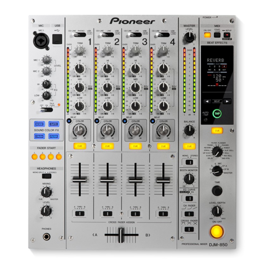
Pioneer DJM-850-K Service Manual
Hide thumbs
Also See for DJM-850-K:
- Operating instructions manual (84 pages) ,
- Operating instructions manual (84 pages) ,
- Operating instructions manual (32 pages)
Table of Contents
Advertisement
Quick Links
DJ MIXER
DJM-850-K
DJM-850-S
THIS MANUAL IS APPLICABLE TO THE FOLLOWING MODEL(S) AND TYPE(S).
Model
DJM-850-K, DJM-850-S
DJM-850-K, DJM-850-S
DJM-850-K, DJM-850-S
DJM-850-K, DJM-850-S
DJM-850-K, DJM-850-S
PIONEER CORPORATION
PIONEER ELECTRONICS (USA) INC. P.O. Box 1760, Long Beach, CA 90801-1760, U.S.A.
PIONEER EUROPE NV Haven 1087, Keetberglaan 1, 9120 Melsele, Belgium
PIONEER ELECTRONICS ASIACENTRE PTE. LTD. 253 Alexandra Road, #04-01, Singapore 159936
PIONEER CORPORATION
Type
Power Requirement
SYXJ8
AC 220 V to 240 V
UXJCB
AC 120 V
LXJ
AC 110 V to 120 V or 220 V to 240 V
KXJ5
AC 220 V
XJCN5
AC 220 V to 240 V
1-1, Shin-ogura, Saiwai-ku, Kawasaki-shi, Kanagawa 212-0031, Japan
2012
DJM-850-K
K-MZV MAR.
ORDER NO.
RRV4298
Remarks
2012 Printed in Japan
Advertisement
Table of Contents

Related Manuals for Pioneer DJM-850-K


Summary of Contents for Pioneer DJM-850-K
- Page 1 PIONEER CORPORATION 1-1, Shin-ogura, Saiwai-ku, Kawasaki-shi, Kanagawa 212-0031, Japan PIONEER ELECTRONICS (USA) INC. P.O. Box 1760, Long Beach, CA 90801-1760, U.S.A. PIONEER EUROPE NV Haven 1087, Keetberglaan 1, 9120 Melsele, Belgium PIONEER ELECTRONICS ASIACENTRE PTE. LTD. 253 Alexandra Road, #04-01, Singapore 159936...
-
Page 2: Safety Information
PIONEER Service Manual. A subscription to, or additional copies of, Also test with plug reversed Earth PIONEER Service Manual may be obtained at a nominal (Using AC adapter ground charge from PIONEER. plug as required) -
Page 3: Table Of Contents
10.9 MAIN ASSY (3/19)..............................114 10.10 MAIN ASSY (4/19)..............................116 10.11 MAIN ASSY (5/19)..............................118 10.12 MAIN ASSY (6/19)..............................120 10.13 MAIN ASSY (7/19)..............................122 10.14 MAIN ASSY (8/19)..............................124 10.15 MAIN ASSY (9/19)..............................126 10.16 MAIN ASSY (10/19)..............................128 DJM-850-K... - Page 4 11.1 INPUT, MIC1 and MTRM ASSYS ..........................168 11.2 MAIN ASSY................................172 11.3 SEC/HP, USBI and HPJK ASSYS..........................178 11.4 PNLA ASSY ................................182 11.5 PNLB and FADC ASSYS ............................186 11.6 FAD1 to FAD4 and REG ASSYS..........................190 11.7 TRANS, PRIMARY and ACSW ASSYS ........................192 12. PCB PARTS LIST ................................196 DJM-850-K...
-
Page 5: Service Precautions
The settings are stored in Flash ROM (IC2802) on the MAIN Assy. To display the [USER SETUP] screen, hold [SETUP (WAKE UP)] pressed for at least 1 sec. To display the [CLUB SETUP] screen, press [POWER] (ON) while holding [SETUP (WAKE UP)] pressed. DJM-850-K... -
Page 6: Specifications
For connection with an unbalanced input (such as RCA), use the [MASTER2] terminals. Accessories • Driver software CD-ROM (DXX2694) • USB cable (DDE1128) • Power cord (SYXJ8, LXJ: ADG7062) (UXJCB: DDG1108) (KXJ5: ADG7115) (XJCN5: ADG7105) • Operating instructions (SYXJ8: DRB1604, DRB1605) (UXJCB: DRB1606) (LXJ: DRB1607) (KXJ5: DRB1608) (XJCN5: DRB1609) DJM-850-K... -
Page 7: Basic Items For Service
Part No. Purpose of use / Remarks USB cable GGP1193 for PC connection Lubricants and Glues List Name Part No. Remarks Silicon grease GEM1057 Refer to "9.3 BOTTOM SECTION". Lubricating oil GYA1001 Refer to "9.4 CONTROL PANEL SECTION (1/2)". DJM-850-K... -
Page 8: Pcb Locations
2..PRIMARY ASSY (SYXJ8, KXJ5, XJCN5) DWR1519 2..PRIMARY ASSY (UXJCB) DWR1520 2..FAD1 ASSY DWX3366 2..PRIMARY ASSY (LXJ) DWR1509 2..FAD2 ASSY DWX3367 2..FAD3 ASSY DWX3368 2..PNLB ASSY DWX3365 2..FAD4 ASSY DWX3369 2..MIC1 ASSY DWX3371 2..FADC ASSY DWX3370 2..MTRM ASSY DWX3372 1..PNLA ASSY DWX3359 DJM-850-K... - Page 9 DJM-850-K...
-
Page 10: Block Diagram
HP_L_OUT GNDD_REFB_PA GNDHP GNDHP CN8001 CN7002 GNDD GNDHP GNDHP KM200NA3 KM200NA3L HP_MIX PHONES HP_R_OUT HP_R_OUT CROSS_FADER 3 V+3R3REF2 3 V+3R3REF2 2 VR_CFD 2 VR_CFD HP_LEVEL 1 GNDREF2 1 GNDREF2 V+3R3_REFA_PA LEVEL_DEPTH PF04PP-S05 GNDD_REFA_PA L=50mm PF03PP-B07 BOOTH_LEVEL L= 75mm V+3R3_REFB_PA DJM-850-K... - Page 11 (DWR1512: LXJ) V-HP_AC V-HP_AC B13B-EH JP3105 P=2.5mm DE007WF0 SEC/HP ASSY CN5001 P=2.0mm 52147-1010 52147-1010 (DWR1511) V+5A_UNREG V+5A_UNREG GND5A_UNREG GND5A_UNREG GND5A GND5A REG ASSY V+5A V+5A V-15A V-15A V-15A_UNREG V-15A_UNREG (DWR1510) GNDA_UNREG GNDA_UNREG GND_PO GND_PO V+15A_UNREG V+15A_UNREG V+15A 10 V+15A DJM-850-K...
-
Page 12: Audio System Block Diagram
ADAT_USBIN 2 differential 90 ADAT_USBIN 2 CH 1 4 USB Ucom ADAT_USBIN 3 ADAT_USB ADAT_USBIN 3 ADAT_USBIN 4 ADAT_USB ADAT_USBIN 4 IC2603 ADSP - BF 525BBCZ - 5A- K ADAT_USB USB_S_CLK 106.5MHz SDRA M (64M) IC2604 16bit M12L64164A- 5TG 2M- DJM-850-K... - Page 13 TURN_ DA C NJM4565MD NJM4580D HEA D ADAT_HP IC1001 AK 4382AVT PHO NES (T RS) ADAT_UDOUT 1 IN 1 ADAT_USB 1 IN 2 ADAT_UDOUT 2 ADAT_USB 2 IN 3 ADAT_UDOUT 3 ADAT_USB 3 IN 4 ADAT_UDOUT 4 ADAT_USB 4 DJM-850-K...
-
Page 14: Dsp Block Diagram
BEAT EFFECT (Others) Effect SW Effect CH Select SEND BEAT Effect CH Select Effect CH Select Level Depth EFFECT Effect Out No Cable Effect SW Return Effect CH Select Level Effect Out RETURN Effect_C Cable Exist Cable Check Effect_C DJM-850-K... - Page 15 Effect CH Select CHx_CUE Effect Out Effect Cue On/Off SW Mixing Effect_CUE Mono Split H.P. MIX L Out Effect_C Stereo MONO SPLIT/ STEREO SWITCH MIXING 2Position Mono Split Master Master Cue On/Off SW Mixing H.P. MIX R Out Stereo Master_CU DJM-850-K...
-
Page 16: Power Block Diagram
/ 16V 3300uF 100uF NJM 7915FA / 35V / 25V V-15A (for Opamp) V- 15A_UNREG TH 2 Poly V-15A (for Opamp [INPUT]) P101 V+HP_UNREG Poly V+HP_UNREG_1 (for HP_Tr) 1000uF / 25V 1000uF V- HP_UNREG / 25V V- HP_UNREG_1 (for HP_Tr) DJM-850-K... - Page 17 DJM-850-K...
-
Page 18: Diagnosis
NEC_B_CTRL setting to LOW Inhibiting and cancelling SUB UCOM from accessing FPGA DIT, DAC reset cancel Loading of setup data power supply, voltage check Notifying of version (Initialization completion) Obtaining KEY data Operation mode judgment Notifying of operation mode DJM-850-K... - Page 19 Standby for USB UCOM version response Notifying of USB UCOM version Notifying of completion of normal DSP startup Initialization process of MAIN UCOM Entering main loop Entering main loop Notifying of completion of input selector, automatic start information USB communication start MUTE setting OFF DJM-850-K...
-
Page 20: Troubleshooting
• If the IC103_1 pin is high level, go to [6]. ————— error IC2803 pin 90 • If the IC103_1 pin is not high level, the RESET IC (IC2801) block may be defective. Check for the status of soldering and replace it. DJM-850-K... - Page 21 IC. Check for the status of soldering and replace it. SUB UCOM PNLA Assy If the symptom persists after the above SUB UCOM (IC6601) may be defective. ————— defective IC6601 corrections. Replace it. DJM-850-K...
- Page 22 The unit is shut down in error by the Voltage Monitoring Circuit. Cause Diagnostics Point Item to be Checked Corrective Action Reference Power failure See “5.4 VOLTAGE Check for power at each point, following Repair the defective parts. 5.4 VOLTAGE MONITORING “5.4 VOLTAGE MONITORING CIRCUIT.” MONITORING CIRCUIT.” CIRCUIT DJM-850-K...
- Page 23 • If Pin 4 is not normal for CH1/CH3 or if Pin 13 1-33 is not normal for CH2/CH4, and if there is no abnormality in the path from the FPGA (IC3007) to IC3006/IC3004/IC3005, soldering of the FPGA (IC3007) or this IC itself is defective. DJM-850-K...
- Page 24 INPUT Assy Check that the RETURN IN signal level • If it is L, JA4401 or R4803 must be ————— /defective parts CN4803 pin 20 is H. improperly soldered or defective. • If it is H, go to [2]. DJM-850-K...
- Page 25 Check for the CLK signal at DA converter. • If the CLK signal is output, soldering of the 1-52 1-53 1-54 pin 6 IC201 or the IC itself is defective. 1-52 6M CLK: IC201 pin 7 1-53 24M CLK: IC201 pin 14 1-54 DJM-850-K...
- Page 26 (C553, C554, C555 and C556), output resistor (R542, R545, R548 and R551) is defective or one or more of those parts is defective. Or the MUTE circuited is activated. • If the MUTE circuited is activated, go to [17]. DJM-850-K...
- Page 27 • If Pin 1 is not normal and if there is no pin 1, pin 3 1-57 abnormality in the path from the FPGA 24M CLK: IC3005 (IC3007) to IC3006/IC3004/IC3005, soldering pin 1, pin 3 of the FPGA (IC3007) or this IC itself is 1-58 defective. DJM-850-K...
- Page 28 • If all signals are normal, soldering of the DIT 1-88 pin 26 (IC3405) or the IC itself may be defective. ADAT_DOUT_FPGASRC Check the soldering status. If soldering is OK, pin 28 1-89 replace the defective part. FPGASRC_MCLK pin 30 1-90 DJM-850-K...
- Page 29 2 Connection between the external device control CD or VINYL (media on which timecodes are recorded) is available. (DJ player, turntable) and the DJM-850 is not properly made. → Check the connection and check if the RCA cables are broken. DJM-850-K...
- Page 30 Replace it. 1-99 Representative CH1 0 to 10. • If no signal is output, the FPGA (IC3007) • Check for the FADER_STOP signal must be improperly soldered or defective. when the CH FADER is changed from 10 to 0. DJM-850-K...
-
Page 31: Power Supply Diagnosis Information
(V+3R3D_*) V+34D 31 to 36 (V+34D_*) V+3R3D_REFA 3.15 to 3.45 CH1-4 FADER, CROSS FADER (V+3R3D_REFA_*) V+3R3_REFB 3.15 to 3.45 (V+3R3D_REFB_*) V+3R3D_REFA 3.15 to 3.45 CROSS FADER (V+3R3D_REFA_*) ex) V+15A_* • • • • V+15A_O, V+15A_IN, etc • • • DJM-850-K... -
Page 32: Voltage Monitoring Circuit
Identify which power-supply IC is defective, by turning the unit OFF then back ON while monitoring each voltage with an oscilloscope. Check the value of each voltage immediately before stopping power supply. Note: Each time before turning the unit ON, make sure that each power-supply IC is not short-circuited to GND. DJM-850-K... - Page 33 3.65 V Short-circuiting at GND or different power supply More than 4.01 to 6.72 V 6.22 V Short-circuiting at regulator (IC1402) IN/OUT V+3R3A − 1.12 to 1.95 V or less 1.29 V Short-circuiting at GND or different power supply DJM-850-K...
-
Page 34: About Polyswitch
P101: RXEF075P-T Diagnostic procedure when any resettable fuse is activated 1. Unplug the AC power cord. 2. Check for any error, such as short-circuiting or defective parts, in the circuits downstream from the resettable fuse. 3. Repair the detective part. DJM-850-K... -
Page 35: About Protector
I N C 2 0 0 2 A C 1 GNDA_OUT GNDA_OUT P 3 0 2 P 3 0 1 A E K 1 0 7 3 - A A E K 1 0 7 3 - A MASTER1_L_HOT MASTER1_R_HOT DJM-850-K... -
Page 36: Diagnosis
L S C 4 0 8 1 U B ( Q R S ) Discharge circuit V+34C_CONT V+34D GNDD High R 1 4 1 6 Q 1 4 0 3 GNDD L S C 4 0 8 1 U B ( Q R S ) 2 . 2 k GNDD DJM-850-K... -
Page 37: Error Indications
Please update it again. ERROR E008 Lit off USB UCOM BOOT UPDATE error Please update it again. ERROR E009 Lit off SYS Ver. UPDATE error Please update it again. ERROR E000 Lit off Others, the whole error Please update it again. DJM-850-K... -
Page 38: Connection Check With Each Interface
Devices to be added: • Universal Serial Bus controllers USB Composite Device • Under “Sound, video and game controllers” PIONEER DJM-850 USB Audio Device A communication check may be easily performed if connection is made with Device Manager displayed on the PC screen. -
Page 39: How To Confirm The Dvs Signal Route
The Master Out signal will not be output if the MAIN volume control is set to the minimum volume position. If the MAIN volume indicators are not displayed on the screen, set the TRAKTOR screen to Full screen. [Connection Diagram (When the CDJ Player is Connected to CH1)] DJM-850 DJM-850 Computers USB cable Power amplifier CDJ player DJM-850-K... - Page 40 Start up the "DJM-850 Settings Utility". (Reference) For Windows Click [Start] menu → [All Programs] → [Pioneer] → [DJM-850] → [DJM-850 Settings Utility]. For MacOS Click [Macintosh HD] → [Aplications] → [Pioneer] → [DJM-850] → [DJM-850 Settings Utility]. MIXER INPUT...
- Page 41 1 After starting TRAKTOR, set the deck layout, in "Mixer". Figure of TRAKTOR2 screen image 2 Set the deck A to D, in "Live Input". Figure of TRAKTOR2 screen image 3 Select Traktor then Preferences, or click on the "Preferences" button. Figure of TRAKTOR2 screen image DJM-850-K...
- Page 42 8 Play the Audio signal of a Player connected to the Mixer, and confirm that a sound is output by the MASTER output. The TRIM knob, Channel Fader, MASTER LEVEL knob of the input path do operation like normal mixer use. Figure of TRAKTOR2 screen image DJM-850-K...
-
Page 43: Ic Information
V+3R3E Power supply (Connect to 3.3 V) − P110/ANO0 USB_ERR_MAIN Error signal from USB − P111/ANO1 VDET Power supply abnormality detection − AVREF0 V+3R3D_REFA Power supply (Connect to 3.3 V) Note "−": There is no built-in pulling up function DJM-850-K... - Page 44 REGC Regulator output for internal working − GNDD Ground − EVSS0 GNDD Ground − V+3R3E Power supply (Connect to 3.3 V) − EVDD0 V+3R3E Power supply (Connect to 3.3 V) Note "−": There is no built-in pulling up function DJM-850-K...
- Page 45 − AVREF1 V+3R3D_REFB_PA Reference power supply for DAC − P110/ANO0 BEAT_DOWN Beat down key input − P111/ANO1 BEAT_UP Beat up key input − AVREF0 V+3R3D_REFB_PA Reference power supply for AD Note "−": There is no built-in pulling up function DJM-850-K...
- Page 46 Regulator output for internal working, be connected to Vss through a capacitor. − GNDD Ground − EVSS0 GNDD Ground for port − V+3R3D_PA Power supply − EVDD0 V+3R3D_PA Power supply for port Note "−": There is no built-in pulling up function DJM-850-K...
- Page 47 USB0_ID Not used (open) USB0_VBUS Not used (open) AMUTE1/EHRPWMTZ/GP4[14] Not used (open) AFSX0/GP2[13]/BOOT[10] McASP0 transmit frame sync UART1_TXD/AXR0[10]/GP3[10] Not used (open) AXR0[6]/RMII_RXER/ACLKR2/GP3[6] CH2 USB IN AXR0[2]/RMII_TXEN/AXR2[3]/GP3[2] CH4 USB IN EMB_CS[0] SDRAM chip select EMB_A[0]/GP7[2] SDRAM address EMB_A[4]/GP7[6] SDRAM address DJM-850-K...
- Page 48 SDRAM data bus EMB_D[31] Not used (open) EMB_D[16] Not used (open) EMB_D[2]/GP6[2] SDRAM data bus RTC_XI Power supply 1.2 V RTC_XO Not used (open) JTAG test clock USB0_VSSA33 Not used (open) USB0_VDDA33 Not used (open) CVDD Power supply 1.2 V DJM-850-K...
- Page 49 Power supply 3.3 V CVDD Power supply 1.2 V DVDD Power supply 3.3 V DVDD Power supply 3.3 V EMB_CAS SDRAM column address strobe EMB_D[22] Not used (open) EMB_D[23] Not used (open) EMA_CAS/EMA_CS[4]/GP2[1] Not used (open) AXR1[9]/GP4[9] SEND OUT DJM-850-K...
- Page 50 Not used (open) SPI1_ENA/UART2_RXD/GP5[12] For DSP processing cycle measurement SPI0_ENA/UART0_CTS/EQEP0A/GP5[3]/BOOT[3] For SPI communication SPI0_SOMI[0]/EQEP0I/GP5[0]/BOOT[0] BOOT mode setting/ For SPI communication EMA_OE/UHPI_HDS1/AXR0[13]/GP2[7] FPGA connection EMA_BA[0]/LCD_D[4]/GP1[14] Not used (open) EMA_A[1]/MMCSD_CLK/UHPI_HCNTL0/GP1[1] External address EMA_A[5]/LCD_D[2]/GP1[5] External address EMA_A[9]/LCD_HSYNC/GP1[9] External address EMA_CLK/OBSCLK/AHCLKR2/GP1[15] Not used (open) DJM-850-K...
- Page 51 Not used (open) SPI0_CLK/EQEP1I/GP5[2]/BOOT[2] BOOT mode setting/ SPI CLOCK SPI1_CLK/EQEP1S/GP5[7]/BOOT[7] BOOT mode setting EMA_CS[3]/AMUTE2/GP2[6] FPGA connection EMA_CS[0]/UHPI_HAS/GP2[4] Not used (open) EMA_A[0]/LCD_D[7]/GP1[0] External address EMA_A[4]/LCD_D[3]/GP1[4] External address EMA_A[8]/LCD_D[3]/GP1[4] External address EMA_SDCKE/GP2[0] Not used (open) EMA_D[0]/MMCSD_DAT[0]/UHPI_HD[0]/GP0[0]/BOOT[12] External data bus EMA_D[9]/UHPI_HD[9]/LCD_D[9]/GP0[9] External data bus DJM-850-K...
- Page 52 USB data line (Differential +) PF0/PPI D0/DR0PRI /ND_D0A Audio input (CH1) PPI_FS1/TMR0 Not used VDDEXT Power supply voltage for I/O USB_DM USB data line (Differential -) PG15/TFS0A/HOST_CE USB_RCV: UART receive information (MAIN) PPI_CLK/TMRCLK Not used VDDEXT Power supply voltage for I/O DJM-850-K...
- Page 53 Power supply voltage for I/O VSS (Ground) VSS (Ground) VSS (Ground) VSS (Ground) VSS (Ground) VDDINT Power supply voltage for internal core VPPOTP Power supply voltage for one time programming AMS3~ Not used PG5/TMR1/PPI_FS2 Not used PG6/DT0PRIA/TMR2/PPI_FS3 Not used DJM-850-K...
- Page 54 Data bus JTAG clock ABE0~/SDQM0 SDRAM data mask ABE1~/SDQM1 SDRAM data mask DATA14 Data bus DATA13 Data bus DATA11 Data bus DATA09 Data bus DATA07 Data bus DATA05 Data bus DATA03 Data bus DATA01 Data bus BMODE3 Boot mode judgment DJM-850-K...
- Page 55 Data bus BMODE2 Boot mode judgment BMODE0 Boot mode judgment ADDR19 Address bus ADDR17 Not used ADDR15 Not used ADDR13 Not used ADDR11 Not used ADDR09 Address bus ADDR07 Address bus ADDR05 Address bus ADDR03 Address bus VSS (Ground) DJM-850-K...
-
Page 56: Service Mode
FADER SOUND (Rear panel) START Mode 4 COLOR Mode 11 Test Mode POWER ON CH-1 (Mode 1) Mode 5 NOISE Mode 10 Mode 8 Mode 7 Mode 6 Test Mode : CANCEL (Rear panel) POWER SW POWER OFF DJM-850-K... - Page 57 BEAT BEAT BEAT d button d button d button BEAT BEAT BEAT c button c button c button Software Name FL Display System MAIN UCOM SUB UCOM DSP (program) DSP (data) USB UCOM FPGA BOOT DJM-850-K...
- Page 58 BEAT EFFECT ON/OFF button BEAT EFFECT ON/OFF button LED EFXon CH1 BEAT button CH1 BEAT button LED CF_B1 CH2 BEAT button CH2 BEAT button LED CF_B2 CH3 BEAT button CH3 BEAT button LED CF_B3 CH4 BEAT button CH4 BEAT button LED CF_B4 DJM-850-K...
- Page 59 CH4 Channel Level Indicator LED selector switch : Right -24dB -15dB -10dB -7dB 1, 2, 3, 4, MIC, CF.A, CF.B, Master Level Indicator ED MASTER selector switch L CH : MIC -5dB : CF.A -3dB : CF.B -2dB : MASTER -1dB DJM-850-K...
- Page 60 This mode is also used to check operation of the TIME control. The value displayed on the FL display increases/decreases as you turn the TIME control: Minimum value Initial value Maximum value Operation range Initial value: 0 Maximum value: 100 Minimum value: -100 Turn Turn counterclockwise. clockwise. DJM-850-K...
- Page 61 Correspondence diagram of Mode 5 : SELECT SW Operating test. "SW TEST" DJM-850-K...
- Page 62 EQ HI control Master Level Indicator L LED "+12": Full Illuminate "-12": Lights off EQ LOW control Master Level Indicator R LED "+12": Full Illuminate "LOW": Lights off CH1 COLOR control At the bottom of the FL display "HIGH": Full Illuminate DJM-850-K...
- Page 63 MASTER LEVEL control Master Level Indicator L LED "0": Full Illuminate "L": Lights off BALANCE control Master Level Indicator R LED "R": Full Illuminate "LOW": Lights off CH3 COLOR control At the bottom of the FL display "HIGH": Full Illuminate DJM-850-K...
- Page 64 "MIN": Lights off LEVEL/DEPTH control Master Levele Indicator R LED "MAX": Full Illuminate "LOW": Lights off CH4 COLOR control At the bottom of the FL display "HIGH": Full Illuminate : Group 1 : Group 2 : Group 3 : Group 4 DJM-850-K...
- Page 65 CH2 CUE button CH2 Channel Level Indicator LED CH3 CUE button CH3 Channel Level Indicator LED CH4 CUE button CH4 Channel Level Indicator LED MASTER CUE button Master Level Indicator L LED EFFECT CUE button Master Level Indicator R LED DJM-850-K...
- Page 66 If the CUE button is pressed while the last VR on each group list is displayed, the top VR on that group list will then be displayed. When the BEAT c, d button is pressed for a layer lower than the 2nd one, the top VR on the list of the next group will be displayed. DJM-850-K...
- Page 67 "-∞": 000 LEVEL control HP_LV "0": 3FF *As an AD value that is displayed on the FL display is the one before a hysteresis removal process, and as it has an amplitude, an error of about ±2 may be produced. DJM-850-K...
- Page 68 "MIN": 000 LEVEL/DEPTH control LV/DP "MAX": 3FF *As an AD value that is displayed on the FL display is the one before a hysteresis removal process, and as it has an amplitude, an error of about ±2 may be produced. DJM-850-K...
- Page 69 FL Display Name Remarks "0": 000 CH1 Channel Fader "10": 3FF "0": 000 CH2 Channel Fader "10": 3FF "0": 000 CH3 Channel Fader "10": 3FF "0": 000 CH4 Channel Fader "10": 3FF "A": 000 Cross Fader CROSS "B": 3FF DJM-850-K...
- Page 70 CH3 CUE EQ LOW HP LEVEL LEVEL/ MASTER DEPTH BALANCE CH1 CUE CH2 CUE CH4 CUE CH3 CUE Mode 11 : AD values of the fader test. "FDR AD" BEAT BEAT BEAT BEAT CROSS FADER FADER FADER FADER FADER DJM-850-K...
-
Page 71: About The Device
M12L64164A-5TG2M IC2604 MAIN Assy SUB UCOM LED, FL, KEY, VR control DYW1809 IC6601 PNLA Assy Two or more FLASH and SDRAM are mounted in this unit. Please judge the device which you should diagnose in reference to this list. DJM-850-K... -
Page 72: Disassembly
White White White Slider Knob 2 Black Gray Black White White Projection Slider Knob 1 FX SEL Knob Knob (TIME) Rotary Knob (BN) (DAA1213) ×1 (DAA1214) ×1 (DAA1220) ×1 Black White White Slider Knob Stopper Black Black Black Gray DJM-850-K... - Page 73 (1) Remove the two knob/MIC. ×2 ×2 (2) Remove the two screws. (BBZ30P060FTB) Knob/MIC (3) Remove the two screws. (BBZ30P060FTC) (4) Remove the two screws. (BPZ30P120FTB) ×2 (5) Remove the six screws. (K: DBA1290, S: DBA1436) ×3 ×3 ×2 Screw tightening order DJM-850-K...
- Page 74 Nut tightening order Tighten the nuts after tightening the screws indicated in the figure on the left. ×2 (6) Remove the MIC1 Assy. MIC1 Assy (7) Remove the two screws. (BBZ30P060FTC) (8) Remove the MTRM Assy with stay. MTRM Assy DJM-850-K...
- Page 75 (12) Lift up the INPUT Assy to a front direction. PNLA Assy Control panel section Diagnosis MAIN Assy PNLB Assy INPUT Assy ACSW Assy FADC Assy HPJK Assy SEC/HP Assy REG Assy PRIMARY Assy TRANS Assy DJM-850-K...
- Page 76 (Positioning of the MAIN Assy is determined by its Bracket PSW attachment position on the rear panel.) MAIN Assy Rear panel Screw tightening order (SEC/HP, REG Assy) Screw tightening order (Stay/INP) MAIN Assy SEC/HP Assy REG Assy Stay/INP DJM-850-K...
- Page 77 2: Be sure to clamp the cables to the Locking Wire Saddle so that they are styled coming from the coil side toward Power level select SW the side of the product, as shown in the figure above. Side panel R (Only LXJ model) DJM-850-K...
- Page 78 Slider knob 2 *: During reassembly, fully push down Slider knob 2 until it is Tweezers Protective material dented into Slider knob 1. 4 Remove the slider knob 1. 5 Remove the slider knob stopper. Slider knob 1 Slider knob stopper DJM-850-K...
- Page 79 (6) Disconnect the four connectors. (CN7201, 7401, 7601, 7801) (7) Release the jumper wire from clamper. • Connectors color Match the color of a connected connector. ×4 ×2 CN8001 FAD1 FAD4 (White) (Yellow) FAD2 FAD3 (Red) (Blue) FADC Assy DJM-850-K...
- Page 80 Style the cable (yellow) from the FAD4 Assy so that it is placed between the PNLB Assy and the FAD3 Fader section and will not protrude from the bottom of the PNLB Assy. (FAD3 Fader section) FAD4 Assy PNLB Assy PNLB Assy • Bottom view PNLB Assy Cable (yellow) DJM-850-K...
- Page 81 10 to 20 strokes, in order to fully spread the grease. Top & Bottom Top & Bottom [3-3] PNLA and PNLB Assemblies (1) Remove the 30 flange nuts M9. ×30 (2) Remove the one nut. DJM-850-K...
- Page 82 (7) Remove the 13 screws. (BBZ30P060FTC) (8) Remove the barrier/A and barrier/PNL. ×13 Barrier/PNL (9) Remove the seven screws. (BBZ30P060FTC) (10) Remove the one screws (PBH30P080FTB) (11) Remove the PNLA and PNLB Assemblies. PNLA Assy ×7 PNLB Assy • Bottom view DJM-850-K...
- Page 83 Be sure to insert this bending part of the barrier into the slit of the Barrier/PNL. Be sure that each FFC is separately placed up and down with regard to the above raising tab and that they do not overlap. DJM-850-K...
-
Page 84: Each Setting And Adjustment
2. [DJM-850_update_manual.pdf] Macintosh: [DJM-850_vxxx_MAC] folder is generated. 1. [DJM-850_vxxx.app] 2. [DJM-850_update_manual.pdf] Notes: • The above xxx denotes the version of new firmware. • The extension (.exe or .upd) may not be displayed, depending on the setting of the computer. DJM-850-K... - Page 85 (No need to update it if current version shows as x.xx. It is the latest firmware.) 1 Connect your computer with DJM-850 by USB cable. 2 Press [CUE (BEAT EFFECT)] button and [ON/OFF (BEAT EFFECT)] button with power button. 3 Check the current version. DJM-850-K...
- Page 86 If the version on the FL display of DJM-850 is displayed with x.xx, the update is completed normally. [Reference information] The update tool is available by the following OS's. Windows: WindowsXP/Windows Vista/Windows 7 Mac: OS X 10.5/OS X 10.6/OS X 10.7 Be approximately 3 minutes at update time. DJM-850-K...
-
Page 87: User Setable Items
48kHz 96kHz MASTER ATT. -6dB -3dB MIDI Button Type Auto Standby TALK OVER MODE Mic Output To Booth Monitor TALK OVER LEVEL -24dB -18dB -12dB -6dB PC Utility Factory Reset NEVER perform FACTORY RESET before taking note of setting data. DJM-850-K... -
Page 88: Exploded Views And Parts List
For the applying amount of lubricants or glue, follow the instructions in this manual. (In the case of no amount instructions, apply as you think it appropriate.) 9.1 PACKING SECTION SYXJ8 only KXJ5 only SYXJ8, UXJCB only SYXJ8, UXJCB only DJM-850-K... - Page 89 16 Packing Sheet RHC1023 NSP 17 Leaflet/NI DRM1367 18 Label/NI See Contrast table (2) (2) CONTRAST TABLE DJM-850-K/SYXJ8, UXJCB, LXJ, KXJ5, XJCN5, DJM-850-S/SYXJ8, UXJCB, LXJ, KXJ5 and XJCN5 are constructed the same except for the following: DJM-850-K DJM-850-K DJM-850-K DJM-850-K DJM-850-K...
-
Page 90: Exterior Secion
9.2 EXTERIOR SECION Refer to "9.4 CONTROL PANEL SECTION (1/2)" . UXJCB only UXJCB UXJCB, LXJ, KXJ5 only only UXJCB only LXJ only LXJ only UXJCB Refer to only "9.3 BOTTOM SECTION" . DJM-850-K... - Page 91 See Contrast table (2) 24 Panel/USB DNK6120 25 Knob/POW See Contrast table (2) (2) CONTRAST TABLE DJM-850-K/SYXJ8, UXJCB, LXJ, KXJ5, XJCN5, DJM-850-S/SYXJ8, UXJCB, LXJ, KXJ5 and XJCN5 are constructed the same except for the following: DJM-850-K DJM-850-K DJM-850-K DJM-850-K DJM-850-K...
-
Page 92: Bottom Section
9.3 BOTTOM SECTION PNLA CN6602 PNLA INPUT CN6601 CN4802 USBI HPJK CN3801 CN9201 INPUT CN4803 INPUT CN4801 Silicon grease (GEM1057) Bottom side LXJ only UXJCB only LXJ only LXJ only DJM-850-K... - Page 93 VNE2489 39 Screw PPZ30P080FTB NSP 19 Spacer AEB7092 20 Spacer DEB1998 (2) CONTRAST TABLE DJM-850-K/SYXJ8, UXJCB, LXJ, KXJ5, XJCN5, DJM-850-S/SYXJ8, UXJCB, LXJ, KXJ5 and XJCN5 are constructed the same except for the following: DJM-850-K DJM-850-K DJM-850-K DJM-850-K DJM-850-K Mark Symbol and Description...
-
Page 94: Control Panel Section (1/2)
After applying grease, move the slider base back and forth from one end to the other for approximately 10 to 20 strokes, in order to fully spread the grease. Nut: Attached part of Rotary encoder Refer to "9.5 CONTROL PANEL SECTION (2/2)" . DJM-850-K... - Page 95 23 Knob (MA) DAA1210 24 Knob (Black) DAA1212 25 FX SEL Knob DAA1213 (2) CONTRAST TABLE DJM-850-K/SYXJ8, UXJCB, LXJ, KXJ5, XJCN5, DJM-850-S/SYXJ8, UXJCB, LXJ, KXJ5 and XJCN5 are constructed the same except for the following: DJM-850-K DJM-850-K DJM-850-K DJM-850-K DJM-850-K...
-
Page 96: Control Panel Section (2/2)
9.5 CONTROL PANEL SECTION (2/2) • Bottom view Note: Refer to “7. DISASSEMBLY” for styling of flexible cables, barriers. MAIN CN1002 MAIN CN1001 Note: Fix the packing/L to the lower right of Barrier FL. Caution: Only this screw is different in a type. DJM-850-K... - Page 97 14 Button/CFX DAC2837 15 Button/CUE DAC2838 16 Button/TAP DAC2839 17 Button/FS DAC2840 18 Button/BFX DAC2841 19 Lens Holder DNK4533 20 Lebel Meter Assy DXB1882 21 Packing/L DEC3416 22 • • • • • 23 Screw BBZ30P060FTC 24 Screw PBH30P080FTB DJM-850-K...
-
Page 98: Schematic Diagram
GND_CH2 Notes is STBY C 4 0 3 6 RS1/10SR***J RS1/8SQ***J 0 . 1 u / 2 5 RN1/16SE****D GND_CH2 V-15A R 4 0 5 0 CCSRCH***J 1 . 2 k CCSQCH***J CCSQ CKSRYB***K CFTLA CFTLA CEANP GND_CH2 CEAT DJM-850-K... - Page 99 : CH1 Audio Signal (L CH) Q 4 0 0 6 L T C 1 1 4 E U B 5:6D (L2) : CH2 LINE Signal (L CH) (CL2) : CH2 CD/LINE Signal (L CH) (C2) : CH2 Audio Signal (L CH) GND_CH2 DJM-850-K...
-
Page 100: Input Assy (2/5)
0 . 0 1 u / 5 0 C 4 2 1 8 GND_CH4 RS1/8SQ***J CFTLA RN1/16SE****D 4 7 0 p / 5 0 1 . 2 k CCSRCH***J CCSQCH***J CCSQ R 4 2 5 7 CKSRYB***K V-15A CFTLA CFTLA CEANP GND_CH4 CEAT GND_P4 DJM-850-K... - Page 101 Q 4 2 0 6 : CH3 Audio Signal (L CH) L T C 1 1 4 E U B 5:8C (P4) : CH4 PHONO Signal (L CH) (CL4) : CH4 CD/LINE Signal (L CH) (C4) : CH4 Audio Signal (L CH) GND_CH4 DJM-850-K...
-
Page 102: Input Assy (3/5)
1 0 0 3 3 k NJM4565MD V-15A C 4 4 0 9 0 . 0 1 u / 5 0 CFTLA Pull up Main side R 4 4 0 1 R 4 4 0 2 STBY GND_RET STBY GND_RET GND_CH4 DJM-850-K... - Page 103 R E T U R N _ R 5:8D R E T U R N _ I N NOTES is STBY RS1/10SR***J RS1/16SS***J RS1/10SR****D RN1/16SE****D CKSRYB CKSSYB CKSYB CFHXSQ CCSRCH CCSSCH CFTLA CEJQ CEANP CEAT CEHAT CEHAZL (RET A) : RETURN Audio Signal (L CH) DJM-850-K...
-
Page 104: Input Assy (4/5)
R 4 6 0 6 O U T Y G N D 2 2 0 GNDD MIDI_OUT TC7SET04FUS1 Q 4 6 0 1 L T C 1 2 4 E U B GNDD GNDD GNDD DNH2736-A / SHIELD CASE(MIDI) GNDD GNDD DJM-850-K... - Page 105 M I D I _ T X D CKSYB 5:6C CFHXSQ CCSRCH CCSSCH CFTLA CEJQ CEANP CEAT CEHAT (MIC1 A) : MIC1 Audio Signal CEHAZL (MIC2 A) : MIC2 Audio Signal : Voltage measuring point : Waveform measuring point DJM-850-K...
-
Page 106: Input Assy (5/5)
R 4 8 1 9 R 4 8 2 7 GND_RET GND_RET GND_CH4 GND_CH4 R 4 8 2 0 R 4 8 2 8 GND_RET GND_RET GND_MIC1 GND_MIC2 R 4 8 2 1 R 4 8 2 9 GND_RET GND_RET GND_MIC1 GND_MIC2 DJM-850-K... - Page 107 : CH3 Audio Signal (L CH) (C4) : CH4 Audio Signal (L CH) (RET A) : RETURN Audio Signal (L CH) (MIC1 A) : MIC1 Audio Signal (MIC2 A) : MIC2 Audio Signal : Voltage measuring point : Waveform measuring point DJM-850-K...
-
Page 108: Mic1 And Mtrm Assys
E Z J Z 1 V 2 7 0 R M CKSQYB V A 9 0 0 2 CFTLA E Z J Z 1 V 2 7 0 R M RS1/10SR****J GNDF GNDA (MIC1 A) : MIC1 Audio Signal DJM-850-K... - Page 109 C K S 3 5 3 3 - A CHASSIS GND GND_MIC1 GND_MIC1 GND_MIC2 MIC2 TRIM (MIC1 A) : MIC1 Audio Signal (MIC2 A) R 8 8 0 2 : MIC2 Audio Signal CHASSIS GND GND_MIC2 NOTES is STBY RS1/10SR***J DJM-850-K...
-
Page 110: Main Assy (1/19)
V R _ F A D E R 1 VR_FADER1 10:12C V+3R3D_REFA GNDD GNDREF_A CN4802 CN4803 V+5D STBY R 1 0 4 6 GNDIN_CH3 (RET A) (RET A GNDD GNDIN_MIC GNDIN_CH1 GNDIN_CH4 GNDIN_CH2 GNDIN_RET (C4) (C3) (C2) (C1) (MIC1 A) (MIC1 A (MIC2 A) (MIC2 A) 1/19 DJM-850-K... - Page 111 5:2B 5/19 To CH2 ADC : Waveform measuring point (C2) CH2_L 5:2E CH1_R 4:2B 4/19 To CH1 ADC (C1) CH1_L 4:2E (MIC1 A) MIC1 8/19 8:8B (MIC2 A) To MIC/RET ADC MIC2 8:8B 1/19 10/19 To MAIN_UCOM MIDI_TXD 10:11A DJM-850-K...
-
Page 112: Main Assy (2/19)
K N 1 2 0 3 K N 1 2 0 5 C K F 1 0 8 9 - A C K F 1 0 8 9 - A C K F 1 0 8 9 - A 2/19 GNDD DJM-850-K... - Page 113 V-15A The > mark found on some component parts : Voltage measuring point indicates the importance of the safety factor of the part. Therefore, when replacing, be sure to use parts : Waveform measuring point of identical designation. 2/19 DJM-850-K...
-
Page 114: Main Assy (3/19)
L S C 4 0 8 1 U B ( Q R S ) V+34C_CONT Discharge circuit V+34D GNDD High R 1 4 1 6 Q 1 4 0 3 GNDD L S C 4 0 8 1 U B ( Q R S ) 2 . 2 k 3/19 GNDD DJM-850-K... - Page 115 : Voltage measuring point CEHVAW***M HVAW Therefore, when replacing, be sure to use parts CEANP***M ( Q R S ) of identical designation. CEANP : Waveform measuring point 3/19 DJM-850-K...
-
Page 116: Main Assy (4/19)
1 0 k (1/2) C 1 6 1 2 (CH1) V+5A_IN STBY R 1 6 1 2 D1604 1 . 1 k C 1 6 0 8 0 . 1 u / 2 5 1SS302 GNDIN_CH1 V-15A_IN GNDA_AD 4/19 DJM-850-K... - Page 117 C 1 6 3 7 GNDA_AD 0 . 0 1 u / 1 6 : Voltage measuring point PCM, left-justified, 24-bit FMT0 Low GNDD FMT1 Low : Waveform measuring point Dual rate ( 64 fS slavemode OSR0 High OSR1 Low OSR2 Low 4/19 DJM-850-K...
-
Page 118: Main Assy (5/19)
(1/2) 1 0 k C 1 8 1 2 (CH2) V+5A_IN STBY R 1 8 1 2 D1804 1 . 1 k C 1 8 0 8 0 . 1 u / 2 5 1SS302 GNDIN_CH2 GNDA_AD V-15A_IN 5/19 DJM-850-K... - Page 119 C 1 8 3 6 GNDA_AD : Voltage measuring point 0 . 0 1 u / 1 6 PCM, left-justified, 24-bit FMT0 Low FMT1 Low GNDD : Waveform measuring point Dual rate ( 64 fS slavemode OSR0 High OSR1 Low OSR2 Low 5/19 DJM-850-K...
-
Page 120: Main Assy (6/19)
1 0 k (1/2) C 2 0 1 2 (CH3) V+5A_IN STBY R 2 0 1 2 D2004 1 . 1 k C 2 0 0 8 0 . 1 u / 2 5 1SS302 GNDIN_CH3 GNDA_AD V-15A_IN 6/19 DJM-850-K... - Page 121 C 2 0 3 5 GNDA_AD : Voltage measuring point PCM, left-justified, 24-bit 0 . 0 1 u / 1 6 FMT0 Low FMT1 Low GNDD : Waveform measuring point Dual rate ( 64 fS slavemode OSR0 High OSR1 Low OSR2 Low 6/19 DJM-850-K...
-
Page 122: Main Assy (7/19)
1 0 k (1/2) C 2 2 1 2 (CH4) V+5A_IN STBY R 2 2 1 2 D2204 1 . 1 k C 2 2 0 8 0 . 1 u / 2 5 1SS302 GNDIN_CH4 GNDA_AD V-15A_IN 7/19 DJM-850-K... - Page 123 C 2 2 3 5 GNDA_AD : Voltage measuring point 0 . 0 1 u / 1 6 PCM, left-justified, 24-bit FMT0 Low FMT1 Low GNDD : Waveform measuring point Dual rate ( 64 fS slavemode OSR0 High OSR1 Low OSR2 Low 7/19 DJM-850-K...
-
Page 124: Main Assy (8/19)
(MIC D) (MIC D) 1-38 1-39 1-37 1-40 C 2 4 1 8 STBY 1 0 0 0 p / 5 0 C 2 4 1 9 GNDA_AD GNDD 0 . 0 1 u / 1 6 GNDD GNDIN_MIC 8/19 DJM-850-K... - Page 125 9 6 k _ C L K _ H P - M I C - R E CCSSCH***D CH (D) 1:6C;5C;11:2L 13/19 To DSP ADAT_MIC_ANA CCSRCH***J SRCH 13:5H (MIC D) CCSQCH***J SQCH CFHXSQ***J CFHXSQ CEVW***M CEVWNP***M CEHVW***M CEHVAW***M HVAW CEANP***M CEANP : Voltage measuring point : Waveform measuring point 8/19 DJM-850-K...
-
Page 126: Main Assy (9/19)
R E S E T B M O D E 2 1 0 : 1 4 F 1 0 0 B M O D E 3 1-16 V+3R3D_ BMODE3-0 : 0100 Boot from SPI host device GNDD GNDD 9/19 DJM-850-K... - Page 127 W 1 0 B M O D E 1 CEVWNP***M GNDD B M O D E 2 CEHVW***M : Voltage measuring point B M O D E 3 CEHVAW***M HVAW CEANP***M CEANP : Waveform measuring point V+3R3D_USB GNDD 9/19 DJM-850-K...
-
Page 128: Main Assy (10/19)
R E L A Y _ C O N T Q 2 8 0 3 L T C 1 2 4 E U B 2 : 3 B 15/19 10/19 GNDD To OUTPUT IF C P U _ M U T E 1 5 : 2 F DJM-850-K... - Page 129 V + 1 R 2 D _ C O N T 3:9B V + 3 R 3 D _ C O N T To POWER 3:9C V + 5 D _ C O N T 3:9E V + 3 4 D _ C O N T 3:2H 10/19 1-71 DJM-850-K...
-
Page 130: Main Assy (11/19)
6 M _ C L K _ H P - M I C - R E GNDD 1:6C;8:11C;8:5C BOARD IF 2 4 M _ C L K _ H P - M I C - R E 1:6C;8:11C;8:5C GNDD 11/19 DJM-850-K... - Page 131 FOR DSP : Voltage measuring point R 3 0 7 7 From To USB UCOM U S B _ S C K 9:2I SPI Boot program 11/19 : Waveform measuring point U S B _ M I S O 9:2I DJM-850-K...
-
Page 132: Main Assy (12/19)
E M B _ D [ 3 1 ] NOTES is STBY RS1/16SS***J RS1/16SS****D RS1/10SR***J SR (D) RS1/10SR****D RS1/8SQ***J RS1/4SA***J RN1/16SE****D RAB4CQ***J CKSSYB***K CKSRYB***K CKSQYB***K CCSSCH***J CCSSCH***D CH (D) CCSRCH***J SRCH CCSQCH***J SQCH CFHXSQ***J CFHXSQ CEVW***M CEVWNP***M CEHVW***M CEHVAW***M HVAW CEANP***M CEANP 12/19 DJM-850-K... - Page 133 P L L 0 _ V S S A BLM31PG601SN1 K 1 1 C V D D 1 9 C V D D 2 0 R S V 1 GNDD R S V 2 : Voltage measuring point 12/19 : Waveform measuring point DJM-850-K...
-
Page 134: A 10.19 Main Assy (13/19)
A D A T _ U S B I N 2 From USB 9:2H (CH3 U/D IN) A D A T _ U S B I N 3 9:2H 9/19 (CH4 U/D IN) A D A T _ U S B I N 4 9:2H 13/19 DJM-850-K... - Page 135 A D A T _ U S B 2 O U T To USB_UCOM 9:2H (CH1 U OUT) A D A T _ U S B 1 O U T 9:2H 1 0 0 : Voltage measuring point 13/19 : Waveform measuring point DJM-850-K...
-
Page 136: Main Assy (14/19)
6 M _ C L K _ D I G I 11:2C (DIG OUT) (DIG OUT) From DSP A D A T _ D O U T 13:15H 17pin C 13/19 Software mode non pull up Hardware mode pull up GNDD 14/19 DJM-850-K... - Page 137 RS1/10SR***J SR (D) RS1/10SR****D RS1/8SQ***J RS1/4SA***J RN1/16SE****D RAB4CQ***J CKSSYB***K CKSRYB***K CKSQYB***K ull up CCSSCH***J CCSSCH***D CH (D) CCSRCH***J SRCH CCSQCH***J SQCH CFHXSQ***J CFHXSQ CEVW***M CEVWNP***M CEHVW***M CEHVAW***M HVAW : Voltage measuring point CEANP***M CEANP 14/19 : Waveform measuring point DJM-850-K...
-
Page 138: Main Assy (15/19)
Q 2 0 3 1-68 L T C 1 2 4 E U B STBY From BOARD IF M V R _ M U T E 1:4B 1/19 GNDD Audio Q203 Q204 MUTE ON 15/19 GNDD MUTE OFF V-15A DJM-850-K... - Page 139 F A D E R _ S T A R T 4 11:6K Q 2 1 0 Audio Q203 Q204 L T C 1 2 4 E U B : Voltage measuring point 15/19 : Waveform measuring point GNDD GNDD GNDD V-15A DJM-850-K...
-
Page 140: Main Assy (16/19)
R 3 0 8 R 3 2 4 R 3 4 0 C 3 2 2 3 . 3 k 2 . 7 k 0 . 1 u / 2 5 V-15A_O GNDA_OUT GNDA_OUT GNDA_OUT MASTER 2R+ (MA2) MASTER 2L+ 16/19 DJM-850-K... - Page 141 : MASTER2 OUT Signal (L ch) CCSRCH***J M A S T E R 2 _ L + SRCH 17:2B CCSQCH***J SQCH CFHXSQ***J CFHXSQ CEVW***M : Voltage measuring point CEVWNP***M CEHVW***M : Waveform measuring point CEHVAW***M HVAW 16/19 CEANP***M CEANP DJM-850-K...
-
Page 142: Main Assy (17/19)
1 0 u / 1 6 3 . 3 k 2 . 7 k 2 . 4 k STBY R 4 3 8 Q 4 1 0 GNDA_OUT GNDA_ 1/19,15/19,16/19,18/19,19/19 From OUTPUT IF M U T E 1:9B;15:3F;16:7E;18:2D;19:4E 17/19 DJM-850-K... - Page 143 R 4 1 6 1/2W CEANP***M CEANP V-15A_O GNDA_OUT GNDA_OUT GNDA_OUT R 4 1 7 Q 4 0 6 : Voltage measuring point I N C 2 0 0 2 A C 1 1 8 k : Waveform measuring point 17/19 GNDA_OUT DJM-850-K...
-
Page 144: Main Assy (18/19)
R 5 4 0 1 0 u / 3 5 3 . 3 k CCG1236-A GND_PO Q 5 1 6 V-15A_O I N C 2 0 0 2 A C 1 R 5 8 4 4 7 k GNDA_OUT 18/19 DJM-850-K... - Page 145 Q 5 1 6 I N C 2 0 0 2 A C 1 1 1 k C 5 6 4 0 . 1 u / 2 5 GNDA_OUT GNDA_OUT A_OUT : Voltage measuring point V-15A_O : Waveform measuring point 18/19 DJM-850-K...
-
Page 146: Main Assy (19/19)
From OUTPUT IF 1:9B;15:3F;16:7E;17:2H;18:2D CKSSYB***K CKSRYB***K CKSQYB***K CCSSCH***J CCSSCH***D CH (D) CCSRCH***J SRCH (SEND D) CCSQCH***J : SEND OUT Digital Signal SQCH CFHXSQ***J (SEND) CFHXSQ : SEND OUT Signal (L ch) CEVW***M CEVWNP***M CEHVW***M CEHVAW***M HVAW CEANP***M CEANP 19/19 DJM-850-K... - Page 147 I C 6 0 2 1/4W NJM4565MD SEND R V-15A_O R 6 2 6 1 8 k GNDA_OUT Q 6 0 4 I N C 2 0 0 2 A C 1 GNDA_OUT GNDA_OUT : Voltage measuring point : Waveform measuring point 19/19 DJM-850-K...
-
Page 148: Sec/Hp Assy (1/2)
R B 1 6 0 L - 4 0 D 1 2 R B 1 6 0 L - 4 0 C 1 8 C 2 2 1 0 0 0 p / 5 0 1 0 0 0 p / 5 0 GNDHP V-HP_UNREG DJM-850-K... - Page 149 The > mark found on some component parts RS1/8SQ***J indicates the importance of the safety factor of the part. RS1/4SA***J NREG Therefore, when replacing, be sure to use parts : Voltage measuring point RS1/10SR****D of identical designation. : Waveform measuring point RN1/16SE****D CCSRCH***J CKSRYB***K CEANP CEAT DJM-850-K...
-
Page 150: Sec/Hp Assy (2/2)
T H 1 0 4 GNDA_HP GND_PO V-15A GNDA_HP R 1 2 3 STBY GNDA_HP R 1 2 4 M U T E INC2002 1:10C STBY 1 5 k Q 1 0 4 GNDA_HP R 1 1 9 GNDA_HP GNDHP GNDA_HP DJM-850-K... - Page 151 RS1/10SR****D (HP O) Therefore, when replacing, be sure to use parts : HP OUT Signal (L ch) RN1/16SE****D of identical designation. RS1/8SQ***J : Voltage measuring point CKSRYB***K : Waveform measuring point CCSRCH***J CEANP CEAT DJM-850-K...
-
Page 152: Usbi And Hpjk Assys
L 3 8 0 1 9/19 V+5_SUB D-USB D-USB CN2602 D+USB D+USB V+5VBUS GND_USB STBY STBY GND_USB GNDF K N 3 8 0 1 C K F 1 0 8 9 - A NOTES is STBY RS1/16SS***J CKSSYB***K CCSSCH***J CCSRCH***J SRCH DJM-850-K... - Page 153 V A 9 2 0 1 GNDHP R 9 2 0 8 (HP O) : HP OUT Signal (L ch) C 9 2 0 5 0 . 0 1 u / 5 0 NOTES is STBY RS1/10SR***J CKSRYB***K CFTLA***J GNDF DJM-850-K...
-
Page 154: Pnla Assy (1/2)
K M 2 0 0 N A 3 R K M 2 0 0 N A 3 E K M 2 0 0 N A 3 Y GNDD_REFA_PA GNDD_REFA_PA GNDD_REFA_PA GNDD_REFA_PA S 6 6 3 4 CFX_BEAT_SW4 D S G 1 CN7201 CN7401 CN7601 CN7801 DJM-850-K... - Page 155 D S G 1 0 7 9 - A C 6 6 3 8 : Waveform measuring point CKSRYB GNDD S 6 6 3 4 CCSRCH CFX_BEAT_SW4 CFX_BEAT4 D S G 1 0 7 9 - A CEAT C 6 6 3 9 7801 GNDD DJM-850-K...
-
Page 156: Pnla Assy (2/2)
D 6 7 4 9 KEY_IN6 VR_IN5 1 S S 3 5 2 S6621 S 6 6 2 8 DSH1066-A D S G 1 0 7 9 - A MASTER 1 C2 3 MONO/ST MASTER CUE MONO STEREO KEY_IN7 DJM-850-K... - Page 157 B O O T H _ L E V E L 1:2K L E V E L / D E P T H 1:2K H P _ L E V E L 1:2K H P _ M I X DJM-850-K...
-
Page 158: Pnlb And Fadc Assys
D 7 0 0 1 D 7 0 0 2 D 7 0 0 3 D 7 0 0 4 V+3R3_REFA V+3R3_REFA_PB V+3R3_REFB V+3R3_REFB_PB FADER LED2 FADER LED3 FADER LED4 FADER LED1 GNDD_LED CH FADER LED CIRCUIT (STBY) GNDD_REFA GNDD_REFA_PB GNDD_REFB GNDD_REFB_PB DJM-850-K... - Page 159 V R 8 0 0 1 ER LED4 GNDD_LED GNDD_LED D C V 1 0 0 6 - A CROSS_FADER V+3R3REF2 V+3R3REF2 VR_CFD VR_CFD GNDREF2 GNDREF2 GNDD_REFA_PB GNDF NOTES is STBY RS1/10SR****J CKSRYB : Voltage measuring point CEAT*** : Waveform measuring point DJM-850-K...
-
Page 160: Fad1 To Fad4 Assys
D C V 1 0 2 7 - A FAD4 ASSY (DWX3369) C N 7 8 0 1 KM200NA3Y GNDREF2 VR_FD4 CN6609 V+3R3REF2 V R 7 8 0 1 Yellow D C V 1 0 2 7 - A K L M N DJM-850-K... -
Page 161: Reg Assy
: Waveform measuring point The > mark found on some component parts indicates the importance of the safety factor of the part. Notes Therefore, when replacing, be sure to use parts is STBY of identical designation. CCSRCH***J CKSQYB***K CKSRYB***K DJM-850-K... -
Page 162: Trans, Primary And Acsw Assys
J P 3 1 0 1 DDX1285-A VIOLE NEUTRAL BROW 110V~120V BLUE 220V~240V : Voltage measuring point : Waveform measuring point J P 3 1 0 2 DDX1284-A VIOLE NEUTRAL NOTES is STBY BLUE LIVE CKSRYB P Q R OTHERS DJM-850-K... - Page 163 C 3 1 1 1 0 . 1 u / 5 0 P 3 1 0 2 V-HP_AC X1284-A VIOLET J P 3 1 0 5 EUTRAL DE007WF0 P 3 1 0 5 GNDHP GNDD GNDA MAIN TRANS GNDF BLUE LIVE DJM-850-K...
-
Page 164: Waveforms
INPUT ASSY INPUT SELECT (CD) INPUT SELECT (PHONO) CH1_L, R (CD, LINE) CH1_L, R (PHONO) V: 5 V/div. H: 200 μs/div. V: 5 V/div. H: 200 μs/div. V: 1 V/div. H: 200 μs/div. V: 20 mV/div. H: 200 μs/div. DJM-850-K... - Page 165 VINR+, - MIC1, MIC2 ADAT_BOOTH, REC, MASTER_L, R BOOTH_L, R 1-18 1-34 1-49 1-65 V: 1 V/div. H: 200 μs/div. V: 1 V/div. H: 200 μs/div. V: 5 V/div. H: 2 μs/div. V: 1 V/div. H: 200 μs/div. 1-35 DJM-850-K...
- Page 166 V: 1 V/div. H: 100 ms/div. HP_L+, -, HP_R+, - FPGASRC_MCLK 1-78 1-90 V: 1 V/div. H: 200 μs/div. V: 1 V/div. H: 10 ns/div. DIGITAL OUT D+USB 1-84 1-92 V: 1 V/div. H: 500 ns/div. V: 200 mV/div. H: 100 ns/div. DJM-850-K...
- Page 167 V: 1 V/div. H: 200 μs/div. PNLA ASSY FL_TXD FL_SCK FL_LAT FL_BK 3-13 3-14 3-16 3-16 V: 1 V/div. H: 500 μs/div. V: 1 V/div. H: 500 μs/div. V: 1 V/div. H: 500 μs/div. V: 1 V/div. H: 500 μs/div. DJM-850-K...
-
Page 168: Pcb Connection Diagram
J4105 GND_CH2 J4100 C4037 J4008 C4047 C4050 C4617 J4030 V-15A J4074 J4031 J4017 V+15A C4049 GND_PO GND_MIC2 J4006 V+15A J4069 J4076 GND_CH1 J4106 GND_CH1 J4045 GND_MIC2 J4057 J4075 C4048 C4801 C4802 CN4801 J4037 J4003 GND_MIC2 CN4801 A B C DJM-850-K... - Page 169 J4066 J4046 V-15A GND_CH4 J4099 C4248 J4067 C4250 GND_CH4 GND_CH1 GND_CH2 GND_CH3 GND_RET J4052 J4087 J4089 J4005 J4073 J4007 J4036 J4026 J4060 J4034 [[ G ]] CONTACT UPPER SIDE CN4803 CN4802 CONTACT UPPER SIDE CN4802 CN4803 (DNP2683-C) CN1003 CN1004 DJM-850-K...
- Page 170 : Voltage measuring point : Waveform measuring point Q4202 Q4204 Q4203 Q4201 IC4203 IC4202 Q4205 IC4005 IC4004 Q4006 IC4401 IC4205 IC4204 Q4206 INPUT ASSY SOLDER SOLDER SOLDER PHONO4 LINE3 LINE2 RETURN IC4203 IC4005 IC4004 IC4202 IC4205 IC4204 DWX3362- INPUT CN4803 CN4802 DJM-850-K...
- Page 171 CN8801 COLD CN9001 (DNP2685-C) SOLDER MIC1 DWX3371- (DNP2685-C) Q4002 Q4004 Q4003 Q4001 Q4601 IC4602 Q4005 Q4603 Q4602 IC4004 Q4006 IC4003 IC4002 IC4601 IC4603 MIDI OUT PHONO1 SOLDER SOLDER LINE2 MIC2 IC4004 C4628 IC4003 IC4002 IC4603 IC4601 R4828 CN4801 (DNP2683-C) DJM-850-K...
-
Page 172: Main Assy
SIDE A MAIN ASSY Q3401 IC3405 IC3404 Q513 IC2802 Q515 IC2801 IC502 IC504 Q516 Q514 IC502 IC1406 IC201 IC3203 IC3004 IC3005 IC3204 IC3006 IC3205 IC3008 IC3007 IC3201 IC2602 IC2601 IC2401 IC3202 IC2603 IC2402 IC2605 IC2604 IC1001 IC1408 IC1405 IC1404 DJM-850-K... - Page 173 SIDE A Q305 Q307 Q308 Q306 Q302 Q304 IC401 IC303 IC304 IC602 IC402 Q301 Q303 Q409 Q410 IC301 IC302 IC601 IC1604 IC2004 IC2804 IC1601 IC2001 IC1602 IC2002 IC1802 IC2202 IC1801 IC2201 IC1804 IC2204 Q1402 IC1401 IC1402 IC1403 Q1405 Q1406 (DNP2682-C) DJM-850-K...
- Page 174 1-12 1-31 1-32 1-33 1-99 1-30 1-11 1-10 1-41 1-17 1-16 1-37 1-40 1-39 1-13 1-38 1-35 1-36 1-44 1-34 1-47 1-46 1-45 1-43 1-42 1-69 1-81 1-79 1-14 1-80 1-82 1-91 1-83 1-93 1-92 1-15 1-95 1-78 1-94 DJM-850-K...
- Page 175 1-70 1-77 1-74 1-75 1-50 1-55 1-22 1-54 1-51 1-30 1-24 1-20 1-18 1-41 1-20 1-18 1-40 1-35 1-34 1-47 1-19 1-21 1-21 1-42 1-19 1-81 1-79 1-80 1-28 1-82 1-26 1-27 1-83 1-25 1-23 1-29 1-96 1-78 (DNP2682-C) DJM-850-K...
- Page 176 SIDE B MAIN ASSY Q405-Q408 Q604 Q603 Q401-Q404 Q602 Q601 IC2003 IC1603 IC2203 IC1803 Q1201 IC1409 Q1206 Q203 Q204 Q1404 Q1401 Q1202 Q205 Q1403 Q1208 Q201 Q1207 Q202 Q2804 Q2803 DJM-850-K...
- Page 177 SIDE B : Voltage measuring point : Waveform measuring point Q206 IC202 Q509-Q512 Q207 Q505-Q508 Q2801 IC2803 Q2802 IC1407 Q1204 Q1205 (DNP2682-C) DJM-850-K...
-
Page 178: Sec/Hp, Usbi And Hpjk Assys
SEC/HP ASSY DWR1511- IC102 SEC/HP GNDA_HP Q105 P102 3300 Q106 Q107 Q108 3300uF 6800uF V-HP_UNREG_1 V+HP_UNREG V+HP_UNREG 6800uF V-HP_AC 6800uF BOND 1000uF GNDHP 6800uF 1000uF V+5A_UNREG V-15_AC 1000uF CN101 OPEN SIDE 1000uF OPEN SIDE CN101 CN3101 HPJK ASSY (DNP2683-C) DJM-850-K... - Page 179 SIDE A CN1005 : Voltage measuring point : Waveform measuring point V-15A TH103 GND_PO V+15A GNDD TH104 3300uF BOND 3300uF GNDA_UNREG 3300uF 3300uF 6800uF [[ G ]] NREG V-15_AC (DNP2683-C) CN2602 CN3101 USBI ASSY CN3801 (DNP2682-C) DJM-850-K...
- Page 180 SIDE B SEC/HP ASSY DWR1511- SEC/HP 4.V-15A 3.GND_PO 2.GND_PO 1.V+15A 1.V+5A_UNREG 2.GND5A_UNREG 3.GND5A 4.V+5A 5.V-15A 6.V-15A_UNREG 7.GNDA_UNREG 8.GND_PO 9.V+15A_UNREG 10.V+15A (DNP2683-C) USBI ASSY CN3801 (DNP2682-C) DJM-850-K...
- Page 181 SIDE B : Voltage measuring point : Waveform measuring point Q102 IC101 IC101 DWR1511- Q102 EC/HP Q101 Q103 Q101 Q104 _UNREG A_UNREG _UNREG A_UNREG A_UNREG CN101 HPJK ASSY (DNP2683-C) DJM-850-K...
-
Page 182: Pnla Assy
S6618 S6619 OPEN SIDE CONTACT SIDE CH3 CUE CN6601 CH2 CUE CH1 CUE CN6609 CN6611 DWX3359- S6642 S6643 S6644 S6641 Heat Proof CN6610 PNLA CN6612 Pre-Flux OPEN SIDE CN6601 CN6602 CN6611 CN6610 CN6612 CN660 CN1001 CN1002 CN7201 CN7401 CN7601 DJM-850-K... - Page 183 CENTER CLICK BALANCE VR6619 VR6615 VR6602 D6694 D6601 S6627 X6601 BEAEFECT CUET D6676 D6693 D6675 D6677 D6695 EFFECT S6628 S6618 S6617 SELECT MASTER CUE CH4 CUE H3 CUE S6622 MASTER S6621 MONO/STE (DNP2684-B) Heat Proof Pre-Flux CN6609 CN6603 CN7801 CN7001 DJM-850-K...
- Page 184 R6667 CH3 CUE R6665 EFFECT SELECT MASTER CUE 15.KEY_IN6 14.KEY_MTX4 13.KEY_IN7 MASTER 12.KEY_MTX5 27.LED_OUT15 MONO/STE 11.EFX_ON/OFF 26.LED_MTX_SEL7A 10.GNDD_REFB_PA 25.GND_LED 9.GNDD 24.CH_FADER_LED 8.HP_MIX 23.GNDD S6621 7.CROSS_FADER 22.EFX_CH_SEL 6.HP_LEVEL 21.KEY_IN3 5.V+3R3_REFA_PA 20.ENC1_1 4.LEVEL_DEPTH 19.KEY_IN4 3.GNDD_REFA_PA 18.ENC1_0 2.BOOTH_LEVEL 17.KEY_IN5 1.V+3R3_REFB_PA 16.KEY_MTX3 CN6603 DJM-850-K...
- Page 185 S6618 S6619 S6620 D6753 D6755 D6754 CH1 CUE CH2 CUE CH3 CUE CN6601 D6730 D6729 D6728 D6727 C6601 D6742 S6643 S6642 CN6609 CN6611 UT15 TX_SEL7A S6641 S6644 D6776 DER_LED H_SEL CN6612 CN6610 (DNP2684-B) CN6609 CN6611 CN6602 CN6601 CN6612 CN6610 DJM-850-K...
-
Page 186: Pnlb And Fadc Assys
PNLB ASSY S7008 HEADPHONES MONO STEREO CENTER CLICK D7002 D7001 D7003 VR7002 MIXING S7010 S7011 S7009 THRU THRU THRU J7015 J7010 J7002 GNDD_REFB VR7001 J7012 C7006 C7004 LEVEL White V+3R3_REFB_PB J7003 J7004 NON CLICK V+3R3_REFB_PB J7005 CN7002 FADC ASSY (DNP2683-C) DJM-850-K... - Page 187 EFFECT CH SLECT S7001 VR7004 TIME BOOTH MONITOR S7014 EQ CURVE ISOLATOR D7004 D7003 S7010 S7012 VR7003 LEVEL/DEPTH S7013 THRU THRU CH FADER EQ CURVE 103B CENTER CLICK J7025 PNLB S7015 CROSS FADER EQ CURVE D7007 ¡DWX3365- ¡DWX D7005 (DNP2685-C) DJM-850-K...
- Page 188 VR7004 [[ G ]] BOOTH MONITOR PNLB ¡DWX3365- EQ CURVE S7001 ¡DWX ISOLATOR TIME S7014 D7004 D7002 D7003 THRU THRU CH FADER EQ CURVE S7013 VR7003 S7012 S7010 LEVEL/DEPTH EFFECT ON/OFF S7007 D7007 S7015 CROSS FADER EQ CURVE D7005 DJM-850-K...
- Page 189 VR7002 16.KEY_MTX3 15.KEY_IN6 14.KEY_MTX4 D7002 13.KEY_IN7 D7001 7003 12.KEY_MTX5 11.EXF_ON/OFF 10.GNDD_REFB_PA 9.GNDD THRU VR7001 8.HP_MIX 7.CROSS_FADER 6.HP_LEVEL 5.V+3R3_REFA_PA D7020 4.LEVEL_DEPTH D7015 GNDD_REFB LEVEL S7011 S7009 3.GNDD_REFA_PA 2.BOOTH_LEVEL 3.V+3R3REF2 V+3R3_REFB_PB 1.V+3R3_REFB_PA 2.VR_CFD 1.GNDREF2 THRU V+3R3_REFB_PB (DNP2685-C) CN7002 FADC ASSY (DNP2683-C) DJM-850-K...
-
Page 190: Fad1 To Fad4 And Reg Assys
NJM7 15FA NJM7 15FA BA05T IC5003 FAD2 ASSY CN7401 CN6610 (DNP2683-C) IC5002 IC5003 IC5001 CN7401 FAD2 DWX3367 (DNP2683-C) FAD3 ASSY CN7601 CN6612 CN7601 FAD3 DWX3368 (DNP2683-C) FAD4 ASSY CN6609 CN7801 CN7801 DWX3369 FAD4 (DNP2683-C) K L M N O DJM-850-K... - Page 191 [[ G ]] FAD2 3.V+3R3REF2 DWX3367 VR7401 (DNP2683-C) FAD3 ASSY CN7601 DWX3368 [[ G ]] 1.V+3R3REF2 2.VR_FD3 FAD3 3.GNDREF2 VR7601 (DNP2683-C) FAD4 ASSY CN7801 1.GNDREF2 2.VR_FD4 [[ G ]] DWX3369 3.V+3R3REF2 FAD4 VR7801 (DNP2683-C) K L M N O DJM-850-K...
-
Page 192: Trans, Primary And Acsw Assys
DWR1521-[J]GREEN 2200uF JP3001 J3013 DWR1520-[U]BLUE DWR1509- [L]BLACK DWR1519- [SY][CN][K]RED BOND JP3001 3.V+D_UNREG 2.GND_D 1.RELAY_CTRL [[ G ]] PRIMARY J3008 [L]ONLY LXJ ONLY J3009 [SY][CN][K][U][J] J3012 OTHERS J3011 3.220?`240V CN3003 2.110?`120V [L]ONLY 1.NEUTRAL CN3004 J3007 2.LIVE [SY][CN][K][U][J] 1.NEUTRAL [SY][CN][K][U][J] Q300 DJM-850-K... - Page 193 3001 (DNP2685-C) COLD Q3001 CAUTION REPLACE IC LINKS AS MARKED. UNREG FU1 TYPE No.218.630MXP MFD.BY LITTELFUSE INC. Y_CTRL FU1 T 630mAL 250V 2.NEUTRAL 1.LIVE WHITE J3008 [L]ONLY AC IN [SY][CN][K][U][J] C3002 J3007 H3002 H3001 J3006 630mAL 250V (DNP2685-C) Q3001 DJM-850-K...
- Page 194 SIDE B ACSW ASSY (DNP2685-C) ADD S DJM-850-K...
- Page 195 SIDE B TRANS ASSY (DNP2685-C) PRIMARY ASSY JP3001 COLD JP3001 3.V+D_UNREG 2.GND_D 1.RELAY_CTRL ADD SOLDER PRIMARY ADD SOLDER 3.220?`240V CN3003 2.110?`120V [L]ONLY 1.NEUTRAL CN3004 2.LIVE [SY][CN][K][U][J] 1.NEUTRAL ADD SOLDER (DNP2685-C) DJM-850-K...
-
Page 196: Pcb Parts List
Not used CN3003 Connector (VH) Not used Not used B3P5-VH Mark No. Description Part No. Mark No. Description Part No. IC 4401 NJM4565MD PARTS LIST (DJM-850-K/SYXJ8) IC 4601,4603 NJM4580MD IC 4602 TC7SET04FUS1 INPUT ASSY SEMICONDUCTORS Q 4001-4004,4201-4204 2SK209 IC 4001,4201 NJM4580D... - Page 197 C 4229,4230,4233-4236 CKSRYB104K25 IC 1404 BD9325FJ C 4238,4239,4241,4242 CKSRYB104K25 IC 1405,1408 BD9328EFJ IC 1406 NJM2878F3-33 C 4243,4244,4247-4250 CEAT470M35 IC 1407 S-1132B25-U5 C 4401,4402,4625,4626 CCSRCH101J50 IC 1409,2801 S-80927CNMC-G8X C 4403,4404 CCSRCH102J50 C 4405,4408 CEAT470M25 IC 1602,1801,1802,2001 NJM4580MD C 4406,4407,4602,4611 CKSRYB103K50 DJM-850-K...
- Page 198 JA 401 JACK DKB1083 R 1215 RS1/16SS2000D JA 502,503 HEADPHONE JACK DKN1622 JA 601,602 MIC JACK DKN1614 R 1216 RS1/16SS8200D JA 3401 1P JACK DKB1089 R 1228-1230 RS1/4SA130J KN 201 SCREW PLATE VNE1948 R 1231 RS1/16SS2701D R 1233,1240,1245 RS1/16SS3302D DJM-850-K...
- Page 199 R 3228,3229 RAB4CQ470J C 1403 CEVW101M25 R 3231 RS1/10SR105J C 1409,1438,2801,2809 CKSRYB105K10 R 3240 RAB4CQ102J C 1411,1417,1430,1431 CCSSCH102J50 R 3423 RN1/16SE1802D C 1413,1415,1434 CCG1236 R 3432 RS1/10SR680J C 1416 CEVW101M50 Other Resistors RS1/16SS###J C 1418,1419,1422,1423 CKSSYB104K10 C 1420 CKSSYB223K16 DJM-850-K...
- Page 200 C 2635,2637,2639,2642 CKSSYB104K10 RS1/10SR1302D C 2641,2645,3010-3012 CCSSCH101J50 R 20 RS1/4SA0R0J C 2643,2647,2649 CKSSYB104K10 R 21,24,25,136 RS1/8SQ0R0J C 2646,2648,2653-2657 CKSSYB103K16 R 101-104 RN1/16SE3901D C 2661,2662,2670,2802 CKSSYB103K16 R 105-108 RN1/16SE1502D C 2804,2805 CCSSCH6R0D50 R 109-112 RN1/16SE3301D C 2808,3021,3036,3242 DCH1201 R 114,115 RN1/16SE5601D DJM-850-K...
- Page 201 KM200NA3R C 9205 CFTLA103J50 CN 6611 PLUG (3P) KM200NA3 CN 6612 PLUG (3P) KM200NA3E FL HOLDER DNF1869 PNLA ASSY SEMICONDUCTORS RESISTORS IC 6601 DYW1809 R 6616 RS1/10SR1202F IC 6602-6604 TC74HC4052AF R 6617 RS1/10SR8201D IC 6605 NJM2903M R 6884,6896-6899 RS1/4SA100J DJM-850-K...
- Page 202 PRIMARY ASSY VR 8001 VARIABLE RESISTOR DCV1006 CN 8001 L-PLUG (3P) KM200NA3L SEMICONDUCTORS Q 3001 KTC3209 RESISTORS D 3001 1SS302 All Resistors RS1/10SR###J D 3002 1SS352 D 3003-3006 1SR154-400 MISCELLANEOUS L 3001 FILTER DTL1131 H 3001,3002 FUSE CLIP AKR1004 DJM-850-K...
- Page 203 RS1/10SR330J Other Resistors RS1/10SR####F CAPACITORS C 3001 ACE7027 C 3003 ACG7030 C 3004,3005 CKSRYB473K50 C 3006 CEAT222M25 C 3007 CKSRYB103K50 ACSW ASSY MISCELLANEOUS S 9401 SWITCH DSA1037 MASK DEC3212 JP 9401 CONNECTOR ASSY 2P DKP3847 CAPACITORS C 9401 ACG7030 DJM-850-K...
Need help?
Do you have a question about the DJM-850-K and is the answer not in the manual?
Questions and answers