
Related Manuals for Panasonic KX-T7456


Summary of Contents for Panasonic KX-T7456
- Page 1 ORDER NO. KMS0104564C1 DIGITAL PROPRIETARY TELEPHONE KX-T7456 / KX-T7456B White Version Black Version (for U.S.A.) SPECIFICATIONS...
-
Page 2: For Service Technicians
2001 Kyushu Matsushita Electric Industrial Co., Ltd. All rights reserved. Unauthorized copying and distribution is a violation of law. 1. CAUTION Note: When you note the serial number, write down all 11 digitals. The serial number may be found on the bottom of the unit. 2. -
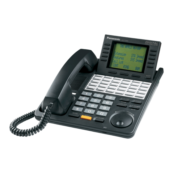
Page 3: Location Of Controls
D100-130, D201, D202) of Main Board, LCD Board. 1) Do not reuse a LED which is removed from the P.C. Board. 2) Use a soldering iron (less than 15 W) for exchanging LED. 3) Do not heat the LED for more than 2 seconds. 4) Do not move the LED after soldering. - Page 4 4. DISASSEMBLY INSTRUCTIONS 4.1. HOW TO REMOVE THE LOWER CABINET (Procedure 1)
- Page 5 (1) Remove the 4 screws A. (2) Remove the lower cabinet. 4.2. HOW TO REMOVE THE HOOK BUTTON (Procedure 1 (1) Remove the hook button. 4.3. HOW TO REMOVE THE SWITCH AND MAIN BOARDS (Procedure 1...
- Page 6 (1) Remove the screws A. (2) Pull out the switch board connector. (3) Remove the switch board. (4) Pull out the flat cable. (See Fig. 1) (5) Remove the 2 screws B. (6) Pull out the speaker and microphone connectors. (7) Remove the main board.
- Page 7 (1) Pull out the flat cable. (See Fig. 1) (2) Remove the LCD block. (See Fig. 2) (3) Remove the 2 screws A. (4) Remove the lower cabinet. (5) Remove the LCD board.
- Page 8 5. IC DATA 5.1. IC1...
- Page 9 Name Dir. Pull Up Type Act. Block Descriptions bidir 8.0mA high PT5B03 Data Bus [3] bidir 8.0mA high PT5B03 Data Bus [2] bidir 8.0mA high PT5B03 Data Bus [1] bidir 8.0mA high PT5B03 Data Bus [0] ADR1 input 12-38k high PT5D01U Address Bus [1] ADR0...
- Page 10 output CMOS 4.0mA PC5O02 0.01 LED Row Drive [5] NROW5 output CMOS 4.0mA PC5O02 0.01 LED Row Drive [6] NROW6 output CMOS 4.0mA PC5O02 0.01 LED Row Drive [7] NROW7 output CMOS 4.0mA PC5O02 0.01 LED Row Drive [8] NROW8 output CMOS 4.0mA...
- Page 12 Name Classification Function APMP Analog Analog Non-invering input terminal of microphone amplifier M1. input Connect to the microphone. Power Reference voltage teminal of DAC. VREFDA supply, etc. Connect the capacitor of 40 F between this terminal (AG2). Ground terminal of the analog circuit. Analog Analog Output terminal for the handset receiver.
- Page 13 Input terminal for PCM data input Output Output terminal for PCM data -FSYNC Input terminal of Sync. signal for PCM interface. The frequency of input sync. input interface signal is 8 kHz. BCLK Input terminal of shift clock pulse for PCM deta. Input pulse frequency renge is 64 kHz~2.048 kHz.
- Page 14 Analog Analog Input terminal of TX microphone signal. input Either this signal or the signal supplied to pin 47 (HI) is AD converter. Power Ground terminal of analog circuit. A5V4 supply, etc. 5V power terminal of analog circuit. AP2HO Analog Output terminal of microphone amplofier H2.
- Page 16 Classification Terminal Pin No. Input/ Function Output Power Power supply terminal supply Ground terminal Input Not the user’s terminal. Connect to the Vcc terminal. Test RESET Input Reset Reset terminal for MCU. OSC1 Input Input/output terminal to the main oscillator. Connect OSC2 Output the ceramic oscillator, crystal oscillator, or external...
-
Page 17: Key Input Control Circuit
6. BLOCK DIAGRAM 7. CIRCUIT OPERATIONS 7.1. KEY INPUT CONTROL CIRCUIT 1) Circuit Operation Sequential input information (negative logic) from the DSHS proprietary telephone is executed by dynamic scanning. The ports RR70 to RR73, RR80 to RR83 of IC6 are brought to low status consecutively. If a key is pressed, the key-in information input is executed by ports R91 to R93, RB1, RB11, RB21, RB0, RD1. - Page 18 1) Circuit Operation The LCD data is output from pins 32 to 35, 40 to 47 and 11 of IC6. LCD contrast adjustment is performed by the circuit composed of Q28, Q29, R109, R108 and R106. The contrast is determined only by the voltage level between V5 and VEE of IC203, IC204 and IC205.
-
Page 19: Led Circuit
7.3. LED CIRCUIT 1) Circuit Operation The LED executes dynamic lighting for the status indicators, and control is executed by the output ports C0 to C5 (column) and R0 to R9 of IC1. A fixed pulse (T=1.82 msec) is output continuously from the/SCK1 terminal of IC9. This pulse is counted and the output of IC1 is shifted sequentially from C0 to C5. -
Page 20: Data Communication Circuit
7.4. DATA COMMUNICATION CIRCUIT 1) Function... - Page 21 The data communication circuit serves the following functions: Information exchanger between the DSHS and DSHS proprietary telephone, key input information as well as data for the LED control, LCD control, etc. This information is continuously exchanged at all times. 2) Circuit Operation When the DSHS propritary telephone receives an IRQ signal from the DSHS and after sending the key input information to the DSHS and receiving data for the LED control, etc., the DSHS proprietary telephone will return to the DSHS an acknowledge signal.
- Page 22 5) IC1 (GATE ARRAY) DPITS Interface DPITS Layer 1 interface. DR [1:0] is receiving input and DX [1:0] is transmitting output. Layer 1 is the transmission method of Ping-Pong type which is AMI encoded. “SYNC/MAM/C/D/ B1/B2/P” data is received in the first half at 125us/frame. After 1 bit time has passed since receiving P data, “SYNC/MAM/C/D/B1/B2/P”...
-
Page 23: Reset Circuit
7.5. RESET CIRCUIT 1) Circuit Operation This circuit is used for transmission of a reset pulse to the CPU (IC6) at the following times, connecting the telephone line jack and circuit operation. The timing chart is shown below. - Page 24 The reset signal is negledted.
-
Page 25: Tone Generation Circuit
7.6. TONE GENERATION CIRCUIT 1) Function Calling tones, Busy tone, DTMF signal and Key in tone are generated in IC2. - Page 26 7.7. JOG DIAL CIRCUIT 1) Circuit Operation This unit is equipped with the JOG switch, which makes the settings of the volume, function selection speed dial, etc. easy and convenient. This JOG switch consists of 2-phase rotary encoder, and the gate array of IC1 counts the number of the rotation to control. The sampling cycle is 1ms and provided with the chattering protective circuit whose available pulse width is 1ms or more.
-
Page 27: Handset Circuit
value is 255. 7.8. HOOK SWITCH CIRCUIT 1) Circuit Operation The hook switch of this unit employs the photo switch consisting of LED and photo transistor. The 2kHz pulse from the gate array of IC2 causes the LED to emit the light. The light is interrupted at ON-HOOK and passes through at OFF-HOOK by the hooking bar,so that the hooking is performed controlling the light of the photo transistor. - Page 28 2) Reception signal path The voice serial data transmitted from PBX is sent to IC1 or IC2 by the serial data. The network control, gain control , A/D conversion is performed in IC2, then the data is output from the handset speaker.
-
Page 29: Troubleshooting Guide
8. TROUBLESHOOTING GUIDE 8.1. NO OPERATION. 8.2. THE LCD DOES NOT OPERATE. -
Page 30: The Electronic Volume Of The Speaker-Phone Does Not Work
8.3. THE ELECTRONIC VOLUME OF THE SPEAKER-PHONE DOES NOT WORK. 8.4. THE ELECTRONIC VOLUME OF THE HANDSET DOES NOT WORK. -
Page 31: Speaker-Phone Trouble
8.5. SPEAKER-PHONE TROUBLE. 8.6. TONE DIAL TROUBLE. 8.7. TROUBLE OF OHCA. -
Page 32: Handset Trouble
8.8. HANDSET TROUBLE. 9. TERMINAL GUIDE OF ICS, TRANSISTORS AND DIODES... -
Page 33: How To Replace The Flat Package Ic
10. HOW TO REPLACE THE FLAT PACKAGE IC If you do not have the special tools (for example: SPOT HEATER) to remove the SPOT HEATER’S Flat IC, If you have solder (large amount) a soldering iron and a cutter knife, you can easily remove IC’s even though large than 100 pin. -
Page 34: Flat Package Ic Remove Procedure
(Original flux should be replaced daily.) 10.2. FLAT PACKAGE IC REMOVE PROCEDURE 1. When all of the IC lead can not been seen at the standard degree, fill with large quantities of solder. Note: If you do not fill with solder and directly cut the IC lead with the cutter, stress may build up directly in the P.C.board’s pattern. -
Page 35: Flat Package Ic Installation Procedure
After removing the Flat IC and when attaching the new IC, remove any of the excess solder on the land using the soldering wire, etc. If the excess solder is not removed from the land, the IC will slip and not be attached properly. 10.3. -
Page 36: Cabinet And Electrical Parts Location
12. CABINET AND ELECTRICAL PARTS LOCATION 13. ACCESSORIES AND PACKING MATERIALS... -
Page 37: Replacement Parts List
14. REPLACEMENT PARTS LIST Note: 1. The marking (RTL) indicates that the Retention Time is limited for this item. After the discontinuation of this assembly in production, the item will continue to be available for a specific period of time. The... -
Page 38: Cabinet And Electrical Parts
retention period of availability depends on the type of assembly and the laws governing parts and product retention. After the end of this period, the assembly will no longer be available. 2. The S mark indicates service standard parts and may differ from production. - Page 39 Ref. No. Part No. Part Name & Description Remarks PSKM1052T1 CABINET, UPPER (WHITE VERSION) PSKM1052T3 CABINET, UPPER (BLACK VERSION) PSGD1026Z CARD, DIAL (WHITE VERSION) PSGD1033Z CARD, DIAL (BLACK VERSION) PSHR1134Z COVER, TEL CARD PQKE82X1 HANGER (WHITE VERSION) PQKE82X2 HANGER (BLACK VERSION) PQHR576Z COVER, TEL NO.
-
Page 40: Main Board Parts
Ref. No. Part No. Part Name & Description Remarks PSGT2177Z NAME PLATE (BLACK VERSION) PSBD1012Z1 COVER, SWITCH 14.2. ACCESSORIES AND PACKING MATERIALS Ref. No. Part No. Part Name & Description Remarks PQJX2PS409Z HANDSET (WHITE VERSION) PQJX2PM409Z HANDSET (BLACK VERSION) PSJA1043Z CORD, HANDSET (WHITE VERSION) PSJA1043Y CORD, HANDSET (BLACK VERSION) - Page 41 Ref. No. Part No. Part Name & Description Remarks PQVTDTD133HK TRANSISTOR(SI) PQVTDTD133HK TRANSISTOR(SI) PQVTDTD133HK TRANSISTOR(SI) PQVTDTD133HK TRANSISTOR(SI) UN5213 TRANSISTOR(SI) UN5213 TRANSISTOR(SI) UN5213 TRANSISTOR(SI) UN5213 TRANSISTOR(SI) UN5213 TRANSISTOR(SI) PQVTDTA143XU TRANSISTOR(SI) 2SC4081Q TRANSISTOR(SI) UN5213 TRANSISTOR(SI) 2SA1576Q TRANSISTOR(SI) UN5213 TRANSISTOR(SI) UN5213 TRANSISTOR(SI) 2SA1576Q TRANSISTOR(SI) PQVTFB1J3P TRANSISTOR(SI)
- Page 42 Ref. No. Part No. Part Name & Description Remarks D122 PSVD2SRVGCT D123 PSVD2SRVGCT D124 PSVD1SRCT D125 PSVD1SRCT D126 PSVD1SRCT D127 PSVD1SRCT D128 PSVD1SRCT D129 PSVD1SRCT D130 PSVD1VGCT (CONNECTORS) PSJP03A05Z CONNECTOR, 3P PSJS36A61Z CONNECTOR, 36P PSJP02A05Z CONNECTOR, 2P PSJP02A05Z CONNECTOR, 2P PSJP04A05Z CONNECTOR, 4P (CERAMIC FILTER)
- Page 43 Ref. No. Part No. Part Name & Description Remarks ERJ3GEYJ330 ERJ3GEYJ472 4.7K ERJ3GEYJ472 4.7K ERJ3GEYJ472 4.7K ERJ3GEYJ472 4.7K ERJ3GEYJ472 4.7K ERJ3GEYJ472 4.7K ERJ3GEYJ122 1.2K ERJ3GEYJ682 6.8K ERJ3GEYJ470 ERJ3GEYJ221 ERJ3GEYJ470 ERJ3GEYJ221 ERJ3GEYJ470 ERJ3GEYJ221 ERJ3GEYJ470 ERJ3GEYJ221 ERJ3GEYJ221 ERJ3GEYJ470 PQ4R18XJ100 ERJ3GEYJ102 ERJ3GEYJ105 ERJ3GEYJ561 ERJ3GEYJ151 ERJ3GEYJ103 ERJ3EKF9102...
- Page 44 Ref. No. Part No. Part Name & Description Remarks ERJ3GEYJ222 2.2K ERJ3GEYJ183 ERJ3GEYJ120 ERJ3GEYJ154 150K ERJ3GEYJ123 ERJ3GEYJ222 2.2K ERJ3GEYJ222 2.2K PQ4R18XJ3R3 ERJ3GEYJ472 4.7K ERJ3GEY0R00 ERJ3GEYJ562 5.6K ERJ3GEYJ104 100K ERJ3GEYJ275 2.7M ERJ3GEYJ562 5.6K ERJ3GEYJ682 6.8K ERJ3GEYJ683 ERJ3GEYJ303 ERJ3GEYJ563 ERJ3GEYJ273 ERJ3GEYJ124 120K ERJ3GEYJ224 220K ERJ3GEYJ104...
- Page 45 Ref. No. Part No. Part Name & Description Remarks R117 ERJ3GEYJ473 R118 ERJ3GEYJ473 R119 ERJ3GEY0R00 R120 ERJ3GEY0R00 R121 ERJ3GEYJ101 R122 ERJ3GEYJ103 R123 ERJ3GEYJ223 R124 ERJ3GEYJ223 R125 ERJ3GEYJ223 R126 ERJ3GEYJ223 R127 ERJ3GEYJ102 R128 ERJ3GEYJ102 R129 ERJ3GEYJ473 R130 ERJ3GEYJ182 1.8K R131 ERJ3GEYJ330 R132 ERJ3GEYJ330 R133...
- Page 46 Ref. No. Part No. Part Name & Description Remarks ECUV1H104ZFV ECUV1H104ZFV PSCEV0JA470 ECUV1H470JCV ECUV1H080DCV 8P ECUV1H104ZFV PQCUV1C334ZF 0.33 PQCUV1C334ZF 0.33 PSCEV0JA220 PQCUV1E104MD 0.1 PSCEV0JA470 PSCEV0JA470 PSCEV1HA100 PSCEV0JA220 PSCEV0JA470 PSCEV0JA471 PQCUV1E681MB 680 PQCUV1C334KB 0.33 PSCEV1HA010 PQCUV1E473MD 0.047 PQCUV1C224KB 0.22 PQCUV1H104ZF 0.1 PQCUV1E104MD 0.1 PQCUV1H153KB 0.015 PQCUV1H473MD 0.047...
- Page 47 Ref. No. Part No. Part Name & Description Remarks PQCUV1H473MD 0.047 PSCEV1HA100 PSCEV0JA220 C106 PSCEV0JA101 C107 PSCEV0JA101 C108 ECUV1H471JCV 470P C111 ECUV1H104ZFV C115 ECUV1H104ZFV C117 ECUV1H104ZFV C118 ECUV1H104ZFV C119 ECUV1H104ZFV C120 PSCEV0JA470 C121 PQCUV1C474ZF 0.47 C122 ECUV1H151JCV 150P 14.4. LCD BOARD PARTS Ref.
-
Page 48: Printed Circuit Board
14.5. SWITCH BOARD PARTS Ref. No. Part No. Part Name & Description Remarks PCB3 PSWP3T7431UK SWITCH BOARD ASS'Y (RTL) (SWITCH) SW301 PSSRCA101Z SWITCH, JOG DIAL (CONNECTOR) CN301 PSJS03Q36Z CONNECTOR, 3P 15. PRINTED CIRCUIT BOARD 15.1. MAIN BOARD (COMPONENT VIEW) 15.2. MAIN BOARD (BOTTOM VIEW) 16. - Page 50 MUTE CO24 CO18 CO12 TRANS D105 D111 D117 D123 D129 D127 C115 C122 R32 R31 CO23 CO17 CO11 PAUSE AUTO FLASH D104 D110 D116 D122 D128 R124 R123 R126 R125 CO22 CO16 CO10 PROG D103 D109 D115 D121 SP-PHONE R147 R145 R152 R148...
- Page 51 R120 R127 D3 D20 D5 D18 D8 D15 R101 R117 R104 R118 R102 C108 R128 R105 GND2 R103 R106 R119 C117 36 35 R133 R107 C120 R108 R110 R114 R109 R100 C119 C118 R139 R140 R121 R131 R132 R122 R135 C112 C113 JP15...
- Page 52 RD[1] IC203 R[91] R[92] 25V4.7µ DIO1 R[93] RB[1] RB[11] RB[21] 100K C204 RD[0] 0.1µ C205 0.1µ C206 0.1µ RR[70-73],RR[80-83] D[2],R[30-33],R[60-63],R[70-73] C203 R205 0.1µ 8 GND R204 D[10] R203 R[33] D[9] 33 R33 R[32] D[5] 34 R32 R140 R[31] 35 R31 36 R40 R139 2.8V...
- Page 53 100K 4.7K 2.2K 0.047 R52 22K 3.9K 120K 1000P 1000P 50V1µ 560K 16V330 µ 120K 0.33 50V10µ 0.068 3.3K 4.7K C114 220K R112 R111 120K 100K 470µ R123 C112 R124 C113 C111 R125 R141 R126 2.2K C121 C110 0.47 R127 6.3V22 µ...
- Page 54 R205 R204 C206 IC201 R201 IC205 C201 R202 C202 C200 D202 C205 IC203 IC204 C204 IC202 IC206 R203 C203 CN201 D201 SW58 SW50 SW59 SW51 SW60 SW52 SW61 SW53 SW62 SW54 SHIFT MENU1 MENU2 MENU3 SW55 SW56 SW57 SW63...
- Page 55 CN301 SW301...
Need help?
Do you have a question about the KX-T7456 and is the answer not in the manual?
Questions and answers